




-
- PCB TYPE
- PRINTED CIRCUIT BOARD PROTOTYPE ALUMINUM PRINTED CIRCUIT BOARD R&F PCB FPC HIGH FREQUENCY PCB HIGH-TG PCB HEAVY COPPER PCB HDI PCB PCB FOR LIGHTING METAL CORE PCB


time:Aug 21. 2026, 10:06:46
In the modern industrial manufacturing ecosystem, electronic hardware reliability directly determines brand reputation, operational uptime, and total product lifecycle costs. Whether engineering high-frequency power controllers, automotive ECU modules, automated robotics gear, or IoT smart grid sensors, original equipment manufacturers (OEMs) face increasing pressure to balance miniaturization with thermal stability and mechanical robustness. At the center of this engineering push sits high-precision circuit board assembly.
Selecting an experienced contract manufacturing partner for printed circuit board assembly involves far more than simply placing components onto bare copper boards. OEM engineering teams and factory procurement leaders require an end-to-end partner capable of resolving component sourcing bottlenecks, executing rigid Design for Manufacturability (DFM) reviews, enforcing strict IPC-A-610 Class 3 compliance, and delivering low-latency production turnaround.
This comprehensive technical guide examines the operational strategies, advanced SMT/THT processes, quality verification protocols, and cost-optimization frameworks required to achieve flawless pcb printed circuit board assembly for industrial applications.
A seamless transition from design layout to full-scale mass production requires an integrated manufacturing workflow. Modern pcb circuit board assembly relies on a closed-loop digital engineering framework where design data, material supply chains, and automated SMT machinery operate in synchronized harmony.
Before any production line is setup, senior NPI (New Product Introduction) engineers inspect the complete engineering package—including Gerber files, ODB++ datasets, IPC-2581 files, and the Bill of Materials (BOM).
Design for Manufacturability (DFM): Evaluates copper weight distribution, line width/spacing, thermal via placement, solder mask clearance, and panelization tab layouts to mitigate board warping during reflow.
Design for Assembly (DFA): Inspects component footprint geometry, pin-1 orientations, component spacing for inspection camera accessibility, and shadow effects caused by tall components adjacent to fine-pitch BGAs.
Solder paste application establishes the structural and electrical foundation for all surface-mount devices (SMDs).
Laser-Cut Nanocoated Stencils: Stainless steel stencils with electro-polished aperture walls and hydrophobic nanocoatings ensure consistent paste release down to 0.3 mm pitch BGA pads.
Fully Automated Solder Paste Printing (SPP): Dual-blade squeegee systems maintain dynamic blade pressure (0.15–0.30 kg/cm) and precise separation speed (0.5–2.0 mm/sec).
3D Solder Paste Inspection (SPI): In-line 3D laser inspection systems measure 100% of printed pads for paste volume, height profile, area coverage, and positional offset before component placement occurs.
Modern high-speed pick-and-place gantry systems handle complex component matrices ranging from ultra-small 01005 passive chips up to 55mm x 55mm fine-pitch System-on-Chips (SoCs). High-resolution vision cameras verify component alignment, ball-grid array pin integrity, and part dimensioning in real time prior to placement.
The populated PCB enters a multi-zone reflow furnace featuring independently controlled heating zones and dual-active cooling stages. Utilizing a closed-loop nitrogen atmosphere (N2 concentration < 500 ppm) drastically suppresses copper oxidation and improves solder wetting on lead-free surface finishes (ENIG, OSP, Immersion Silver).
For heavy-duty industrial assemblies featuring high-power transformers, terminal blocks, large electrolytic capacitors, and rugged I/O connectors, through-hole insertion remains essential. Automated axial/radial insertion equipment combined with selective wave soldering machines deliver precise solder pot thermal transfer without exposing surrounding SMT components to unnecessary thermal stress.
To explore a detailed technical breakdown of every production stage, consult our complete
To meet demanding industrial specifications, modern factory facilities must maintain state-of-the-art SMT and THT machinery capable of executing ultra-dense layout designs under strict dimensional tolerances.
| Engineering Parameter | Standard Industrial Capability | Advanced High-Precision Capability |
| Minimum Component Size | 0201 Imperial (0603 Metric) | 01005 Imperial (0402 Metric) |
| Minimum BGA Pitch | 0.40 mm | 0.30 mm Micro-BGA / PoP (Package on Package) |
| BGA Inspection Technology | 2D Automated X-Ray Inspection | 3D Computed Tomography (CT) X-Ray |
| Maximum Panel Dimensions | 510 mm x 460 mm | 1200 mm x 600 mm (Long-LED & Backplane) |
| Board Thickness Accommodation | 0.4 mm to 3.2 mm | 0.2 mm (Flexible) to 6.0 mm (Heavy Backplane) |
| Plated Through-Hole Aspect Ratio | 8:1 | 12:1 to 16:1 Advanced High-Aspect Vias |
| Maximum Copper Weight | 3 oz (105 µm) | 10 oz (350 µm) Heavy Power Substrates |
| Reflow Soldering Environment | Forced Air Convection | Pure Nitrogen (N2) Purge (< 300 ppm O2) |
| Inspection & Quality Standards | IPC-A-610 Class 2 | IPC-A-610 Class 3 / Space & Automotive |
High-mix, low-to-high volume production lines must adapt to dynamic manufacturing requirements. By integrating multi-function SMT placement heads with real-time feedback sensors, factories eliminate mechanical line re-tooling delays.
Discover how our factory lines support complex multi-layer industrial builds with
In commercial circuit board assembly, high First Pass Yield (FPY) is the cornerstone of cost control and line throughput. Defects discovered after reflow—such as tombstoning, solder bridging, voiding, or pin-hole voids—require manual rework, which introduces thermal risks to surrounding components.
First Pass Yield represents the percentage of assembled circuit boards that pass all functional and visual quality checkpoints without requiring any manual rework or repair:
FPY = (N_pass / N_total) * 100
Where:
N_pass = Total number of defect-free assembled units passing initial inspection.
N_total = Total number of units entering the assembly process line.
To systematically monitor production line quality across diverse product builds, engineering teams track Defects Per Million Opportunities (DPMO):
DPMO = (D / (U * O)) * 1000000
Where:
D = Total number of defects detected across the batch.
U = Total number of assembled units inspected.
O = Total defect opportunities per unit (sum of component leads, solder joints, and placement locations).
Achieving a low DPMO (< 10 DPMO) requires strictly adhering to core DFM/DFA layout rules during the PCB layout phase:
                 CORE DFM / DFA LAYOUT CHECKLIST

1. SOLDER MASK DAM: Maintain minimum 0.05mm mask dam between pads.
2. THERMAL RELIEF: Implement 4-spoke thermal relief on ground planes.
3. COMPONENT CLEARANCE: Keep 0.5mm clearance around fine-pitch BGAs.
4. FIDUCIAL MARKS: Place 3 global fiducials on panel margins.
5. COPPER BALANCE: Ensure equal copper distribution across top/bottom.
Solder Mask Webbing & Dams: Maintain a minimum 0.05 mm (2 mil) solder mask dam between adjacent fine-pitch SMT pads to prevent liquid solder bridges during reflow.
Symmetrical Thermal Relief Layouts: Connect component pads on heavy internal ground or power planes using 4-spoke thermal relief patterns. Asymmetrical heat sinking causes one side of a passive chip to reflow faster than the other, resulting in vertical surface tension imbalance and component tombstoning.
BGA Fan-out & Via-in-Pad Management: When placing vias inside fine-pitch BGA solder pads (Via-in-Pad), always require conductive/non-conductive via filling followed by flat planar capping (IPC-4761 Type VII). Uncapped open vias wick liquid solder down the barrel, causing severe BGA voiding and intermittent open circuits under vibration.
Component availability and authenticity represent major operational risks in the global electronics supply chain. Counterfeit microcontrollers, gray-market passives, and unexpected component obsolescence can halt an entire OEM factory production run.
To protect OEM clients from grey-market risks, top-tier manufacturing partners enforce a rigorous 5-stage material procurement framework:
Direct Original Manufacturer & Franchise Sourcing: 100% of active components (ICs, MOSFETs, SoCs) are sourced directly from tier-1 franchise distributors (e.g., Arrow, Avnet, DigiKey, Mouser) with full Certificates of Conformance (CoC).
Automated BOM Scrubbing & Health Analysis: Before purchasing, procurement systems analyze the complete BOM against global component databases to flag End-of-Life (EOL), Not Recommended for New Designs (NRND), and long lead-time parts.
In-House Quality Counterfeit Testing: Suspicious or hard-to-find components undergo rigorous incoming inspection:
Visual Inspection: Surface blacktopping checks, acetone solvency testing, and pin re-tinning evaluation.
X-Ray Analysis: Verifies internal wire bond distribution and die frame integrity without destroying the component body.
Decapsulation & Die Marking Inspection: Acid decapsulation reveals original semiconductor die logos and wafer manufacturing codes.
When selecting an offshore production facility, verifying vendor supply chain transparency is critical. Learn more by reading our industry evaluation on
In modern NPI cycles and industrial emergency maintenance scenarios, production downtime can cost OEM enterprises tens of thousands of dollars per hour. Achieving rapid turnaround times without sacrificing IPC Class 3 quality requires specialized quick-turn manufacturing infrastructure.
Executing urgent circuit board assembly within 24 to 48 hours requires bypassing traditional batch setup sequences in favor of a synchronized agile workflow:
Dedicated Quick-Turn SMT Production Lines: Quick-turn orders bypass standard mass production queues and land on dedicated NPI assembly lines equipped with modular, quick-change feeder carts and offline programming systems.
Laser Direct Imaging (LDI) & Rapid Stencil Cutting: Fiber-laser stencil cutting systems manufacture stainless steel stencils within 2 hours of Gerber approval.
Pre-Stocked High-Frequency Passive Components: Automated component carousels keep thousands of standard SMD resistors, capacitors, inductors, and common power regulators pre-verified and ready for immediate loading.
Parallel Inspection & Fly-Probe Testing: Instead of building complex hard-wired test fixtures, quick-turn prototypes are instantly verified using high-speed flying probe testers equipped with multi-needle precision measurement probes.
When product launches depend on strict deadlines, leverage ApolloPCB's rapid-response infrastructure with our specialized
Industrial electronics operate under extreme thermal shocks, mechanical continuous vibration, electrical line surges, and humid ambient conditions. A robust quality assurance framework ensures that every assembled circuit board meets strict operational standards before deployment.
Post-reflow 3D AOI systems utilize multi-angle projector arrays and high-resolution top/side camera modules to construct complete 3D topological height profiles of every solder joint. This automated check instantly detects:
Solder volume deficiencies and insufficient fillets.
Component coplanarity issues and lifted leads.
Micro-tombstones, billboarding, and side-mounted chip components.
Polarity reversals and incorrect component laser markings.
Because solder joints underneath BGA, QFN, and LGA packages are invisible to optical cameras, 3D Computed Tomography (CT) X-Ray inspection is essential. Advanced algorithms slice through the chip stack to measure void percentages inside BGA solder balls. Per IPC-A-610 Class 3 specifications, cumulative BGA voiding must remain strictly below 15% of the total pad area.
Electrical testing verifies circuit continuity, resistance values, capacitance tolerances, diode polarities, and component node voltages:
In-Circuit Testing (ICT): Employs a custom "bed-of-nails" test fixture to press hundreds of spring-loaded test pins onto dedicated PCB test points simultaneously, enabling 100% parametric verification of high-volume runs in seconds.
Flying Probe Testing (FPT): Utilizes multiple software-controlled robotic needles to test high-density boards without requiring expensive physical test fixtures—ideal for low-to-medium volume production.
Functional testing simulates actual operational conditions by powering the assembled board and loading firmware, verifying real-time I/O communications (CAN bus, RS485, Ethernet, Modbus), sensor signals, and switching waveforms. Environmental Stress Screening (ESS)—including thermal cycling (-40°C to +125°C) and powered burn-in chamber testing—accelerates latent component failures, guaranteeing rock-solid field reliability.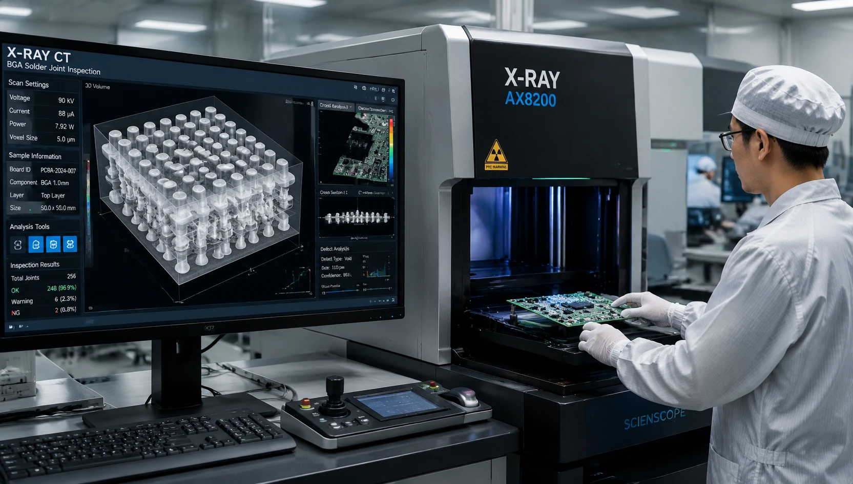
Evaluating the true financial impact of printed circuit board assembly requires looking beyond upfront unit pricing. A cheap initial unit price can quickly become expensive if high field failure rates, component delays, or unexpected engineering NRE charges occur downstream.
Bill of Materials (BOM) Component Cost (60% - 75%): The primary cost driver. Strategic cross-referencing of passive components and pin-compatible IC alternatives can reduce raw material expenditure by 15% to 30%.
SMT Line Setup & Machine Run Time (15% - 25%): SMT machine setup costs are fixed per production run. Increasing panelization density (e.g., placing 6 up or 12 up on a standardized 400mm x 350mm panel sheet) lowers per-unit machine cycle costs significantly.
Tooling, Stencils & NRE Charges (2% - 5%): One-time Non-Recurring Engineering (NRE) fees cover SMT stencil laser cutting, ICT fixture assembly, and pick-and-place machine programming.
Quality Testing & Conformal Coating (5% - 10%): Automated testing (FCT/ICT) adds slight processing overhead but eliminates expensive warranty returns and on-site field repairs.
Standardize Component Footprints: Avoid mixing redundant passive package sizes on a single board (e.g., standardizing on 0603 or 0402 across the entire layout reduces SMT feeder setup changes).
Consolidate SMT Components to One Side: Designing 100% of SMT components on the top layer reduces reflow passes and line handling fees by nearly 50%.
Optimize Panel Edge Fiducials: Provide standard 5mm break-away panel borders with 1.0mm optical fiducial targets to enable high-speed automated machine loading without specialized carrier trays.
Achieving long-term manufacturing success in modern electronics requires a contract assembly partner equipped with advanced SMT facilities, stringent quality verification workflows, and reliable component supply networks.
By integrating multi-zone reflow profiling, 3D SPI/AOI/AXI inspection, and IPC-A-610 Class 3 compliance into every build, ApolloPCB delivers high-yield circuit board assembly tailored to industrial OEM specifications.
Ready to optimize your next production run and reduce time to market? Engineering teams and procurement managers can upload Gerber files and complete BOM files to
ApolloPCB provides rapid 24-hour to 48-hour quick-turn assembly for prototype and urgent production builds, backed by dedicated SMT lines, automated stencil cutting, and in-house component stocks.
Yes, ApolloPCB offers flexible sourcing models including full turnkey (complete BOM procurement and fabrication), partial consignment, and full material consignment based on customer manufacturing needs.
All BGA builds at ApolloPCB adhere strictly to IPC-A-610 Class 2 or Class 3 standards, utilizing 3D Solder Paste Inspection (SPI) alongside 3D Computed Tomography X-Ray (AXI) to guarantee solder voiding remains below 15%.

Got project ready to assembly? Contact us: info@apollopcb.com



 Whatsapp 0086 755 29438407
 Mail info@apollopcb.com
 Tel 0086 755 29438407


ABOUT US

PRODUCTS
TECHNOLOGY
KNOWLEDGE CENTRE
CULTURE
NEWS
We're not around but we still want to hear from you! Leave us a note:

Leave Message to APOLLOPCB
