-
- PCB TYPE
- PRINTED CIRCUIT BOARD PROTOTYPE ALUMINUM PRINTED CIRCUIT BOARD R&F PCB FPC HIGH FREQUENCY PCB HIGH-TG PCB HEAVY COPPER PCB HDI PCB PCB FOR LIGHTING METAL CORE PCB
Real PCB &PCB Assembly Manufacturer
IS09001:2015 Standard
UL.RoHS. REACH Certified
3000+ Orders/Day
99% on-time Shipping
100,000+ Customers
PCB Layout is a two way process. Effective communication between you and us is key to a successful project.
We welcome your questions and suggestions.
How APOLLOPCB work with you
Effective communication is the key to success for the projects.
We appreciate files and main cases through email and details on Skype. Contact information listed on the right upper corner of the sign in page.
What APOLLOPCB need for design&layout?
1)Schematics(.DSN and .SCH suffixes )
2)DXF structure drawing (2D drawing in AutoCAD format, used to position the device and build board size)
3)The component specification (the specification must be with the device size diagram for the establishment and physical one-to-one corresponding package
4)Special requirements
Now we offer "PCB Layout and Design Industrial Design, Electronics Development, 3D Printing Box Build Services, Mold Design and Manufacture, Product Lifecycle Management, Software and Firmware Development" service.

layer definition = unique labeling of each layer leads us how to make your board .
layer orientation = labeling to avoid mirrored layers.
To produce your PCB correctly, it must have a label(name) for each layer.
Even when your data uniquely defines which layer the top or bottom is, the layer orientation for Design Rule should be followed. Many Layout programs permit mirrored data output, so confusion may cause.
View from top side of the design file, we need all top and inner layers in normal vision as the real board, but for all bottom layers, mirrored vision is requested.
Below picture is an example.
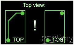
The captions "layer 1" to "layer 4" are shown only for clarity.
PCB panel is a consideration for both PCB manufacturing and PCB assembly cause some boards are irregular. The panel can reduce the time and labor for production and testing.
APOLLOPCB, as the most professional manufacturer in this field for more than a decade. We can make the boards according to your panel design. Also, we can provide the service to help you panel the single board for free.
What is the panel?
That means we help you connect the single boards(same or different are both OK) on one big panel by different route process, then it will be easy for you to break them into single PCB. For the routing process, it has three types: V-scoring, Tab route, and stamp holes
1. V-scoring
Panel with V-Cut/V-Scoring/V-Groove
For V-scoring panelization, space between boards can be 0mm or 3mm. Please take following images as reference.
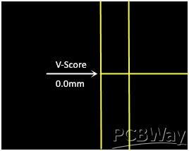
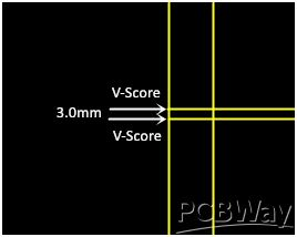
V-scoring has to be continuous and can not be stopped in panel, if you have many different boards like following image to be panelized, we suggest add tab routes between boards instead of V-scoring.
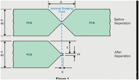
V-scoring is the most popular way in the PCB panel. V-scoring is the v-shape line to connect boards for convenience separation. We also require the v-scoring boards, please observe the following rules
•The gap between the individual circuit boards in the layout is 0mm based on the minimum spacing between copper pattern (trace/pad/copper ground) and V-cut line is 0.4mm.
• Scoring lines must be straight; horizontal and vertical lines are possible, so the board's frame must be regular, and the size of boards must be over 75mm*75mm
• For stability, we recommend using scoring only above a minimum circuit board thickness of 0.4mm
2. Tab route and stamp holes
For tab route and stamp holes, it can be used in the irregular boards. However, For the tab route, the space between boards should be 1.6mm.
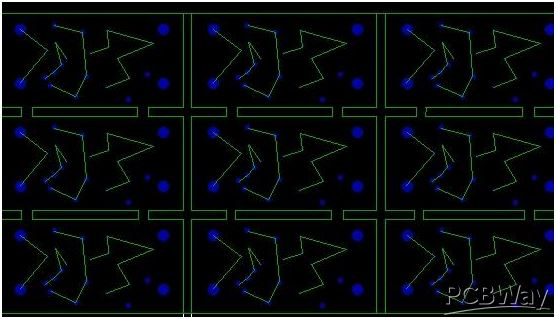
Panel with Tab Route
For panel with tab routes, 1.6mm space is needed between boards. There are 2 kinds of tab routes be used for panel. One is tab route with breaking holes(stamp holes) and the other one is tab route with tab.(no holes).
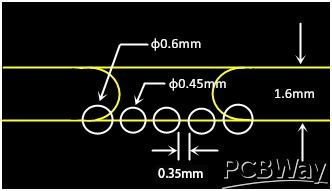
Tab route with breaking holes(stamp holes)
For tab route with breaking holes diameter should be ≥0.45mm, regular diameter is 0.55mm-0.6mm. Holes space has to be ≥0.35mm, usually we will add 5-6 holes to each tab, please take following image as reference.
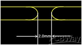
Tab route with tab, tab width has to be at least 2mm, please find following image.
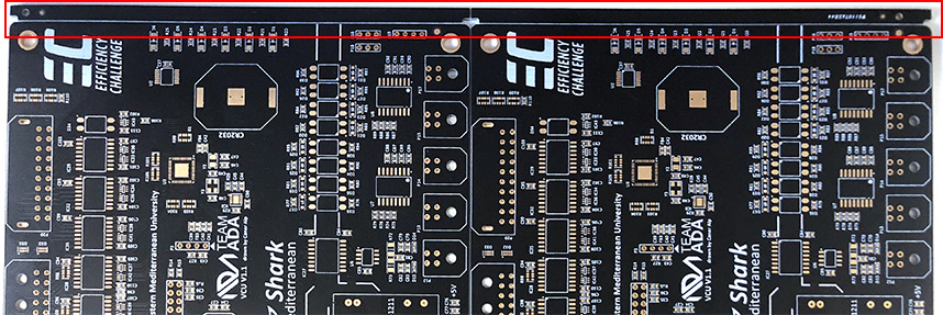
3. Breakaway rails
Breakaway rail, also called edge rail, is a rail at the edge of panel boards to fix the panel boards on a machine more easily. So it is usually used in assembly PCB boards. For breakaway rails, you can also use a v-scoring or tab route to connect then you can cut the rails easily after assembly. In our factory, our mini edge rail is 5mm. Please see the following picture
Advantages
.Mass production. If you need to build a large number of PCBs, panelization will save you time and money.
.Product Safety. Panelization protects the PCB from shock and vibration during assembly.
.Speed and efficiency. From paste printing to component assembly, soldering, and even testing, as part of a large array, processing multiple boards at once is faster and more efficient.

Got project ready to assembly? Contact us: info@apollopcb.com


We're not around but we still want to hear from you! Leave us a note:

Leave Message to APOLLOPCB
