




-
- PCB TYPE
- PRINTED CIRCUIT BOARD PROTOTYPE ALUMINUM PRINTED CIRCUIT BOARD R&F PCB FPC HIGH FREQUENCY PCB HIGH-TG PCB HEAVY COPPER PCB HDI PCB PCB FOR LIGHTING METAL CORE PCB


time:Aug 19. 2026, 16:08:17
In modern industrial hardware design, thermal management remains one of the primary constraints governing power conversion efficiency, component lifespan, and overall system reliability. As switching speeds rise and operational footprints shrink across industrial automation controllers, LED driver arrays, power supplies, and automotive electronics, conventional FR-4 glass-epoxy substrates frequently reach their thermal dissipation thresholds. Conversely, migrating entirely to Aluminum Metal Core PCBs (MCPCBs) often introduces unnecessary material expense, routing constraints, and complex mechanical processing requirements.
To bridge this crucial cost-performance gap, advanced hardware engineering teams rely on thermal cem3 (Composite Epoxy Material 3) laminates. Offering enhanced thermal conductivity ratings alongside superior mechanical punchability and multilayer routing flexibility, high-performance thermal CEM-3 substrates provide OEM factories with a high-reliability, cost-optimized circuit board foundation.
Composite Epoxy Material 3 (CEM-3) represents a hybrid laminate structure engineered to balance the mechanical strength of glass-cloth FR-4 with the processability and thermal properties required for demanding commercial and industrial applications.
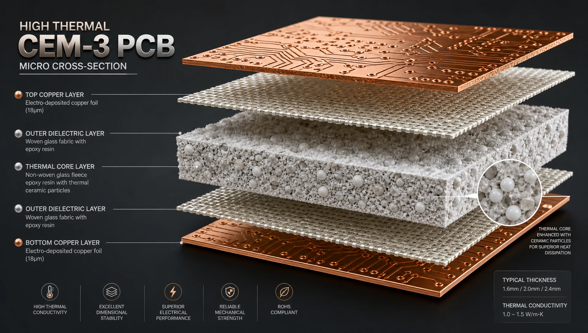
The physical cross-section of a thermal cem3 laminate is constructed from three distinct functional material zones, layered symmetrically to preserve physical flatness and structural equilibrium during high-temperature manufacturing:
Top and Bottom Copper Foils: Standard production accommodates electro-deposited or rolled-annealed copper foils from 0.5 oz (18 µm) to heavy 5 oz (175 µm) weights. High-adhesion silane treatments on the foil surface ensure excellent bond strength to the underlying dielectric.
Surface Woven Glass Fabric Layers: Positioned immediately beneath the outer copper foils, these thin layers utilize fine-weave glass cloth identical to standard FR-4 grade materials. They deliver high flexural strength, superior surface flatness, and robust copper peel resistance under continuous operating vibration.
Central Non-Woven Ceramic-Filled Core: The central core consists of a non-woven glass micro-fleece (glass paper) matrix fully impregnated with an epoxy resin loaded with sub-micron ceramic dielectric fillers, such as micro-silica, alumina, or boron nitride particles. This non-woven construction eliminates directional grain stress, dramatically reduces mechanical drill bit wear, and provides continuous z-axis thermal dissipation channels.
To accommodate varied industrial voltage and heat profiles, specific resin formulations are engineered for targeted operating demands:
st210g High Thermal CEM3 PCB Laminates: Formulated for high-power industrial LED modules and switching power supplies, the st210g high thermal cem3 pcb specification maintains a high Glass Transition Temperature (Tg >= 130°C to 150°C), low z-axis coefficient of thermal expansion, and stable z-axis heat transport under sustained continuous loads.
HA30 High Thermal CEM3 Material: Engineered for high-voltage industrial power converters operating in harsh environments, the ha30 high thermal cem3 material variant integrates elevated ceramic particle loading to achieve enhanced dielectric breakdown voltages (> 45 kV) and a maximum Comparative Tracking Index (CTI 600V, PLC Class 0).
To evaluate comprehensive substrate specifications and custom layer stackup options, explore our specialized
| Performance Property | Standard FR-4 | Standard CEM-3 | High Thermal CEM-3 | Aluminum MCPCB |
| Thermal Conductivity (W/m·K) | 0.2 - 0.3 | 0.3 - 0.5 | 0.8 - 1.5 | 1.0 - 8.0 |
| Glass Transition Temp (Tg °C) | 130 - 140 | 125 - 135 | 140 - 170 | N/A (Polymer Layer 130-150) |
| Comparative Tracking Index (CTI) | CTI 175 - 250 | CTI 250 - 400 | CTI 600 (PLC 0) | CTI 600 (PLC 0) |
| Dielectric Breakdown Voltage (kV) | > 35 | > 35 | > 45 | > 3.0 (AC Insulation) |
| Drill Tool Life (Hits/Bit) | ~1,500 - 2,000 | ~4,000 - 6,000 | ~3,500 - 5,000 | Special Milling / Punching |
| Punchability Rating | Poor | Excellent | Excellent | N/A (Mechanical CNC / Die) |
| Relative Material Cost Factor | 1.0x | 0.85x - 0.95x | 1.1x - 1.3x | 2.2x - 3.5x |
For an in-depth material comparison for industrial electronics, read our comprehensive
Evaluating heat transport through a high thermal cem3 pcb substrate requires analyzing the conductive heat flux through the composite dielectric layer under steady-state operating conditions.
When an active semiconductor device generates heat, thermal energy conducts sequentially along the primary z-axis: moving from the component junction into the top copper pad, passing through the ceramic-filled CEM-3 dielectric matrix, and dispersing into the bottom copper ground plane or attached secondary heat sink.
Thermal conduction through a dielectric substrate is governed by Fourier's Law:
Q = k * A * (T_top - T_bottom) / d
Where:
Q = Heat transfer rate / Dissipated Power (Watts)
k = Thermal conductivity of the substrate (W/m·K)
A = Active heat dissipation surface area (m²)
T_top - T_bottom = Temperature gradient across the substrate layer (°C)
d = Substrate dielectric thickness (m)
The substrate's internal thermal resistance (R_th_sub) measures its opposition to heat flow:
R_th_sub = d / (k * A)
In standard FR-4 (k = 0.25 W/m·K) with a 1.6 mm thickness (d = 0.0016 m) over a 100 mm² thermal pad (A = 0.0001 m²):
R_th_FR4 = 0.0016 / (0.25 * 0.0001) = 64.0 °C/W
By substituting a thermal cem3 substrate with a ceramic-enhanced rating of k = 1.0 W/m·K:
R_th_CEM3 = 0.0016 / (1.0 * 0.0001) = 16.0 °C/W
This structural material change achieves a 75% reduction in dielectric thermal resistance, allowing high-power surface-mount components (MOSFETs, IGBTs, driver ICs, and high-power LEDs) to run at significantly lower operating junction temperatures without requiring expensive thermal interface materials or external metal core structures.
To predict the semiconductor die junction temperature (T_j) on an active board:
T_j = T_a + P_d * (R_th_jc + R_th_cs + R_th_sub + R_th_sa)
Where:
T_a = Ambient operating temperature (°C)
P_d = Power dissipated by the component (W)
R_th_jc = Thermal resistance from junction to component case (°C/W)
R_th_cs = Thermal resistance across the solder joint interface (°C/W)
R_th_sub = Thermal resistance of the thermal CEM-3 substrate (°C/W)
R_th_sa = Thermal resistance of the secondary heat sink to ambient air (°C/W)
By integrating high thermal dielectric substrates, hardware engineers can safely operate industrial devices at higher ambient temperatures while extending mean time between failures (MTBF). For additional thermal modeling insights, consult our detailed analysis on
Beyond heat dissipation performance, thermal cem3 offers major manufacturing advantages during high-volume printed circuit board fabrication and assembly.
Fabricating high-thermal CEM-3 boards follows a streamlined, high-yield manufacturing sequence optimized for high throughput:
Raw Laminate Preparation: High-density CEM-3 panel sheets are trimmed and cleaned under temperature-controlled cleanroom conditions.
Precision Mechanical Processing: CNC drilling machines or mechanical die punches process through-vias, slots, and mounting holes with minimal edge burring.
Chemical Plating & Circuit Etching: Copper walls are deposited via electroless copper plating, followed by photo-imageable etching of circuit traces.
Solder Mask & Surface Finishing: Thermally resistant solder mask inks are applied, followed by high-solderability finishes (ENIG, HASL, OSP).
V-Scoring & Depanelization: Panels undergo automated computer-controlled V-scoring or tab-routing, ensuring smooth board separation during assembly.
Standard FR-4 uses coarse woven glass bundles in both horizontal and vertical directions. As high-speed tungsten carbide drill bits penetrate woven FR-4, the alternating density of glass bundles and epoxy resin causes tool wear, drill deflection, and burring.
In contrast, the non-woven glass fleece core of a high thermal cem3 pcb substrate provides a uniform, homogeneous structure. This results in:
Up to 300% longer CNC drill bit life compared to FR-4 processing.
Lower drill breakages during small-hole fabrication (0.25 mm to 0.40 mm vias).
Reduced micro-burr generation and superior hole wall smoothness for copper plating.
For high-volume single-sided and double-sided power electronics, CNC drilling can become a major production bottleneck. Thermal cem3 substrates exhibit excellent cold-punching properties:
OEM manufacturers can utilize mechanical die stamping for outline blanking, slotting, and mounting hole creation.
Punching reduces mechanical edge fracturing, crazing, and delamination commonly observed in stamped FR-4.
Production throughput increases dramatically while reducing tooling overhead for high-volume production runs.
High-thermal CEM-3 formulations incorporate balanced glass fabric surface layers, controlling thermal expansion across the X and Y axes. During multi-pass lead-free SMT reflow profiling (peak temperatures reaching 255°C - 260°C), thermal CEM-3 maintains tight bow and twist tolerances (<= 0.5%), preventing component tombstoning, solder bridging, and surface-mount pad misalignment.
For detailed guidelines on integrating high-thermal substrates into automated manufacturing, review our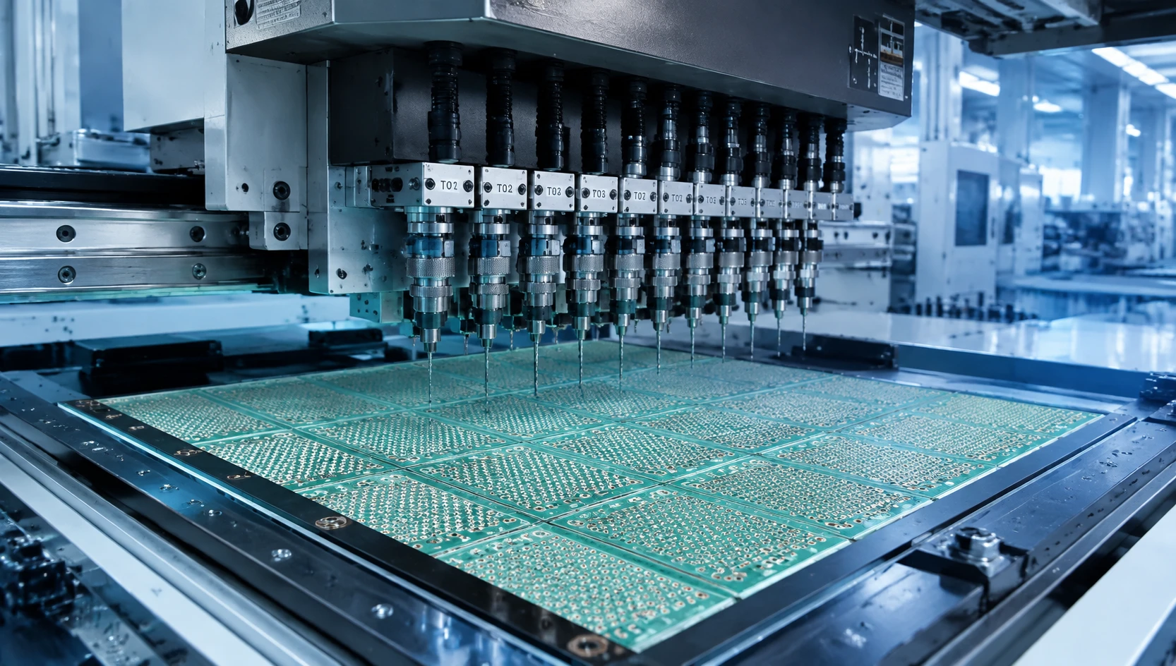
Industrial power supply units, motor drives, smart grid meters, and automotive sub-assemblies operate in harsh electrical and environmental conditions. Substrates must maintain insulation integrity under continuous high voltage, elevated ambient humidity, and thermal cycling.
In high-voltage power circuits, electric fields across adjacent conductors create potential surface arc leakage paths. When surface moisture or airborne particles contaminate standard substrate surfaces, localized electrical tracking can degrade the polymer and form carbon tracks, eventually causing dielectric short circuits.
The enhanced dielectric formulation of thermal cem3 mitigates this failure mechanism by suppressing surface carbon degradation. High dielectric strength ensures that electric fields remain confined safely within copper traces without breaking down the underlying material.
Electrical tracking is the gradual degradation of a dielectric material's surface due to high-voltage stress, moisture, and contamination, leading to conductive carbon paths and catastrophic short circuits.
Standard FR-4 typically achieves CTI Class 3 ratings (CTI 175V to 240V).
Advanced ha30 high thermal cem3 material formulations achieve CTI 600V (PLC Class 0), the highest attainable rating under IEC 60112 testing standards.
A CTI 600V rating allows designers to reduce minimum creepage distance requirements between high-voltage copper traces, enabling compact power supply layouts without sacrificing safety compliance.
Dielectric Strength: Thermal CEM-3 dielectric layers withstand over 45 kV/mm of electrical stress, preventing dielectric puncture in industrial transient surge events.
Flammability Compliance: Impregnated with halogen-free or standard brominated flame retardants, all thermal CEM-3 boards meet UL 94V-0 self-extinguishing safety standards.
To learn more about industrial isolation and compliance criteria, explore our guide on
The technical properties of thermal cem3 make it an ideal substrate across multiple mid-to-high power industrial electronics sectors.
High-power LEDs convert approximately 70% of input electrical energy into heat. Accumulated thermal stress causes luminous flux drop, color temperature shifting, and LED chip failures. Utilizing an st210g high thermal cem3 pcb with 1.2 W/m·K conductivity rapidly draws heat away from the LED pad to the bottom copper plane, maintaining low LED junction temperatures at a fraction of aluminum board costs.
Planar transformers, power MOSFETs, and bridge rectifiers generate localized thermal hot spots while operating on 380V - 480V three-phase AC lines. High thermal cem3 pcb substrate materials provide high z-axis thermal dissipation combined with CTI 600V isolation, allowing high-density power component placement without thermal breakdown or electrical arc tracking.
Under-hood automotive controllers, daytime running light drivers, and cabin climate controls experience continuous thermal cycling (-40°C to +125°C) and severe mechanical vibration. The non-woven fleece core of thermal CEM-3 absorbs mechanical stresses and vibration fatigue better than pure woven glass laminates, mitigating solder joint micro-cracking over extended service lifespans.
To achieve maximum yields and optimal thermal performance on thermal cem3 production lines, PCB layout engineers should apply specific design rules.
When designing active component footprints (such as power MOSFETs or high-current ICs) on thermal CEM-3, placing an array of thermal vias directly beneath the component pad accelerates heat transfer from the top component layer to the bottom copper ground plane:
Thermal Via Grid Arrangement: Position 0.3 mm diameter plated through-holes (PTH) on a tight 0.8 mm to 1.0 mm grid directly under the component thermal pad.
Via Plating Thickness: Maintain at least 25 µm (1 oz) copper wall plating in all thermal vias to maximize vertical thermal conduction.
Capping and Tenting Options: Utilize epoxy-filled and capped vias (IPC-4761 Type VII) to prevent solder wicking away from component leads during SMT reflow.
Heavy Copper Processing: Thermal CEM-3 laminates seamlessly support 2 oz (70 µm) and 3 oz (105 µm) heavy copper foils, accommodating high surge currents in power conversion circuits.
Copper Balance Ratios: Maintain uniform copper density between the top and bottom layers to prevent minor substrate warping during high-temperature reflow passes.
Surface Finishes: Electroless Nickel Immersion Gold (ENIG) and Organic Solderability Preservatives (OSP) are recommended for flat fine-pitch SMT pads. Lead-Free HASL is ideal for heavy industrial power connectors.
Solder Mask Windowing: Open solder mask areas under heat-generating components to allow direct contact with thermally conductive potting compounds or heat sinks.
For factory procurement teams and contract electronics manufacturers (CEMs), material selection impacts both unit pricing and total manufacturing overhead.
High thermal CEM-3 laminates cost approximately 35% to 50% less than aluminum metal core substrates while delivering up to 1.5 W/m·K thermal performance. This material efficiency allows factories to reduce Bill of Materials (BOM) costs without downgrading thermal specs.
Because the non-woven glass core of thermal CEM-3 reduces drill wear by up to 300% and allows high-speed mechanical die punching, factories realize substantial secondary savings:
Reduced tool changeover downtime on automated CNC lines.
Faster mechanical outline processing speeds compared to milling aluminum plates.
Higher panelization yields (exceeding 88% sheet utilization) due to flexible array scoring options.
Selecting thermal cem3 laminates allows engineering teams to resolve mid-tier heat management challenges without incurring the high costs and routing restrictions of metal core boards. Key operational highlights include:
Enhanced Heat Dissipation: Thermal conductivity options ranging from 0.8 W/m·K to 1.5 W/m·K dissipate z-axis thermal energy efficiently.
High Electrical Reliability: CTI 600V tracking resistance and > 45 kV dielectric strength ensure long-term stability in high-voltage industrial environments.
Superior Manufacturing Yields: Uniform non-woven core structures extend drill bit life, enable cold-punching, and maintain board flatness during SMT reflow.
ApolloPCB provides complete fabrication and SMT assembly services for advanced thermal CEM-3, FR-4, and metal core circuit boards. Engineering teams and factory procurement directors can upload Gerber files and BOM specifications to
Thermal CEM-3 provides up to 1.5 W/m·K thermal conductivity at a significantly lower material cost (typically 35% to 50% lower than aluminum MCPCBs). It also supports double-sided component placement and standard V-scoring, whereas aluminum boards are generally restricted to single-sided SMT layouts.
Yes, st210g high thermal cem3 pcb laminates are fully compatible with standard double-sided surface mount technology (SMT) and automated lead-free reflow profile temperatures up to 260°C without bowing, twisting, or delamination.
ApolloPCB manufactures custom thermal CEM-3 boards in multiple thermally enhanced grades ranging from standard 0.5 W/m·K up to high-grade 1.2 W/m·K and 1.5 W/m·K ceramic-filled substrates tailored for high-power industrial applications.

Got project ready to assembly? Contact us: info@apollopcb.com



 Whatsapp 0086 755 29438407
 Mail info@apollopcb.com
 Tel 0086 755 29438407


ABOUT US

PRODUCTS
TECHNOLOGY
KNOWLEDGE CENTRE
CULTURE
NEWS
We're not around but we still want to hear from you! Leave us a note:

Leave Message to APOLLOPCB
