


-
- PCB TYPE
- PRINTED CIRCUIT BOARD PROTOTYPE ALUMINUM PRINTED CIRCUIT BOARD R&F PCB FPC HIGH FREQUENCY PCB HIGH-TG PCB HEAVY COPPER PCB HDI PCB PCB FOR LIGHTING METAL CORE PCB
Real PCB &PCB Assembly Manufacturer
IS09001:2015 Standard
UL.RoHS. REACH Certified
3000+ Orders/Day
99% on-time Shipping
100,000+ Customers
The circuit part and the thermal layer part of the substrate are on different circuit layers, and the thermal layer part directly contacts the heat dissipation part of the lamp bead to achieve the best heat dissipation (zero thermal resistance) effect. And the material of the substrate is generally the copper substrate.
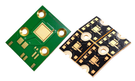
1. Selecting the copper substrate: the density is high, the substrate itself has strong heat carrying capacity, and the heat conduction and heat dissipation are good.
2. Adopting the thermoelectric separation structure: contact the lamp bead with zero thermal resistance, reduce the weakness of lamp bead light and extend the life of lamp bead to an extreme.
3. The density of the copper substrate is high, and the heat carrying capacity is strong, and the volume is smaller under the same power.
4. Suitable for matching single high-power lamp beads, especially COB package, making the lamp to achieve better results.
5. According to different needs, various table treatments (immersion gold, OSP, spray tin, silver plating, immersion silver + silver plating) can be carried out, and the surface treatment layer has excellent reliability.
6. Different structures can be made according to the different design needs of the lamps (copper bumps, copper concave block, paralleled thermal and
Not applicable to single crystal chip bare crystal package.
")
1. First, cut the copper foil substrate to a suitable size for processing.
2. Note that before pressing the substrate, the copper foil on the copper surface need to be roughened by brushing and micro-etching.
3. The Dry film photoresist is adhered to the copper core PCB at an appropriate temperature and pressure, and the photoresist produce polymerization after being irradiated with ultraviolet rays in the light transmitting region of the film (The dry film of the region will be retained as an etch stop in the later step of developing copper-etching.), and the line image on the film will be transferred to the dry film photoresist on the board.
4. After tearing off the protective film on the film surface, using sodium carbonate solution to remove the image develop of unexposed area on the film surface. And then using hydrochloric acid and a mixed solution of hydrogen peroxide to remove the exposed copper foil corrosion to form a line.
5. Finally, using aqueous solution of sodium hydroxide to wash away the dry film photoresist that has been retired. For the inner layer circuit board of six or more layers, using the automatic positioning punching machine to flush out riveting reference hole for alignment of interlayer lines")

Got project ready to assembly? Contact us: info@apollopcb.com


 Whatsapp 0086 755 29438407
 Mail info@apollopcb.com
 Tel 0086 755 29438407


ABOUT US

PRODUCTS
TECHNOLOGY
KNOWLEDGE CENTRE
CULTURE
NEWS
We're not around but we still want to hear from you! Leave us a note:

Leave Message to APOLLOPCB
