




-
- PCB TYPE
- PRINTED CIRCUIT BOARD PROTOTYPE ALUMINUM PRINTED CIRCUIT BOARD R&F PCB FPC HIGH FREQUENCY PCB HIGH-TG PCB HEAVY COPPER PCB HDI PCB PCB FOR LIGHTING METAL CORE PCB


time:Jul 16. 2026, 15:45:16
Global Original Equipment Manufacturers (OEMs), automotive electronics designers, and industrial power infrastructure engineers face a mounting challenge: how to manage extreme thermal profiles and high-current densities within increasingly compressed spatial footprints. Standard printed circuit boards with conventional 1oz or 2oz copper weights routinely fail under these rigorous operating environments, suffering from trace delamination, thermal runaway, and catastrophic electrical arcs.
To mitigate these physical vulnerabilities, modern industrial procurement segments are shifting toward the integration of a heavy copper pcb. By utilizing thick copper distributions—ranging from 3oz up to 20oz or more—these specialized boards serve as both high-current conductors and localized thermal heat sinks.
This comprehensive technical guide provides a deep-dive engineering review of thick copper laminate architectures. We analyze electrical current carrying capacities, specialized DFM (Design for Manufacturability) guidelines, cross-sector applications, and strategic supply chain frameworks that help global factories achieve long-term field reliability while remaining exceptionally cost-effective.
To execute successful engineering deployments, it is vital to establish what distinguishes a heavy copper pcb from its standard thin-film counterparts within commercial fabrication facilities.
In standard circuit fabrication, copper cladding weight is measured in ounces per square foot (oz/ft2). A single ounce translates to an approximate linear thickness of 35 micrometers (um).
The industry broadly categorizes thick copper substrates into two production classifications:
Heavy Copper: Base or plated copper weights tracking between 3oz (about 105 um) and 10oz (about 350 um). The most commonly requested production baselines for standard industrial step-down converters include the 6oz heavy copper pcb and 8oz heavy copper pcb variants.
Extreme Copper: Any board configuration where the interior or exterior copper tracking measures from 11oz up to 30oz (about 1050 um). These are reserved almost exclusively for heavy power grid switches and massive military traction controls.
Standard PCBs rely heavily on simple chemical etching to subtract unwanted copper from a pre-laminated panel. For thick boards, this standard process is insufficient. Achieving a highly reliable thick copper cross-section requires a precise combination of heavy differential etching alongside multi-stage electroplating.
Specialized facilities utilize proprietary plating techniques to add copper thickness inside plated through-holes (PTH) and via sidewalls. This process seamlessly joins high-current surface traces with interior heavy power planes, optimizing overall system performance.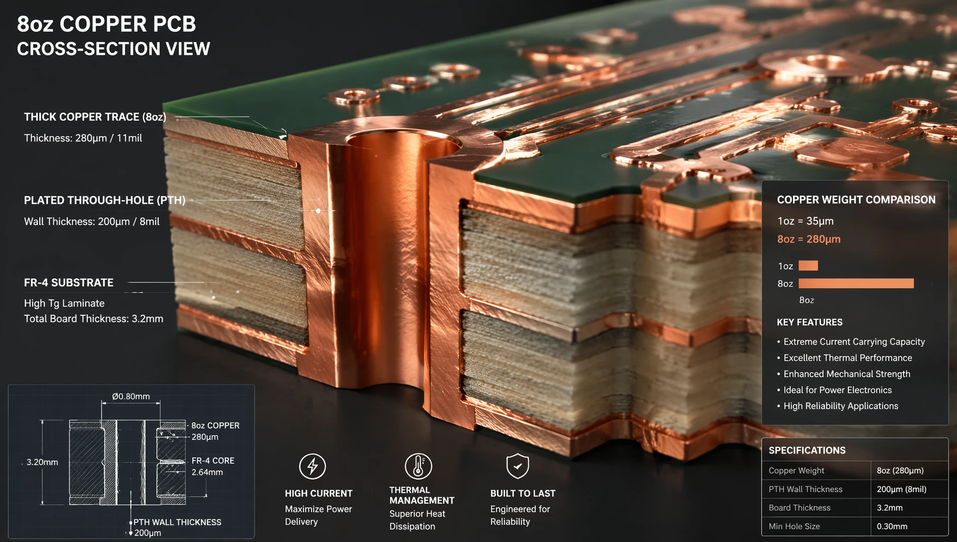
When designing a heavy copper pcb for power supply networks or renewable energy grid inverters, engineers must calculate trace widths based on exact thermal rise parameters rather than arbitrary geometric assumptions.
Thick copper paths lower the overall circuit resistance. This directly minimizes I2R power loss, reducing the amount of waste heat generated when current flows through the system.
The absolute current carrying capacity of a copper conductor is dictated by the cross-sectional area of the trace, the allowable maximum temperature rise (Delta T), and the surrounding ambient environment.
By scaling up the copper thickness from 1oz to an 8oz heavy copper pcb profile, the cross-sectional area increases eightfold without expanding the literal horizontal width of the trace layout on the board surface.
| Design Parameter | Standard 1oz Copper | Heavy 6oz Copper | Heavy 8oz Copper | Industrial Implications for Procurement |
| Trace Thickness (um) | 35 um | 210 um | 280 um | Drastic cross-sectional volumetric expansion within identical board widths. |
| Current Capacity (300 mil width, Delta T = 20 degrees C) | about 15 Amps | about 48 Amps | about 60 Amps | Allows factories to pass large currents through compact modular spaces safely. |
| Thermal Conductivity (Kc) | 390 W/m-K | 390 W/m-K | 390 W/m-K | Fixed material constant, but increased mass accelerates planar heat spreading. |
| Via Wall Plating Thickness | about 25 um | 50 to 75 um | 75 to 100 um | Exceptional mechanical structural reinforcing within thermal vias. |
| Tensile Mechanical Strength | Minimal | Moderate | High | Acts as a rigid physical exoskeleton, resisting high vibrational stresses. |
For a meticulous evaluation of trace width calculation rules and IPC-2152 heat-rise design charts, read our engineering blueprint on
The global heavy copper pcb market is undergoing a period of rapid expansion. This growth is primarily driven by the electrification of commercial transportation, the widespread adoption of high-efficiency renewable energy storage systems, and the modernization of heavy industrial automation grids.
The rapid global transition toward electric vehicles (EVs) and hybrid architectures requires robust onboard power electronics. Engineers rely on a heavy copper pcb for automotive builds to handle demanding applications:
EV Traction Inverters: Converting high-voltage DC power from battery packs into three-phase AC power to drive vehicle motors.
Integrated Power Distribution Assemblies: Replacing bulky, hand-wired wire harnesses and solid copper busbars with structured, multi-layered heavy copper substrates. This significantly reduces overall chassis weight and eliminates manual assembly errors on factory assembly lines.
High-Speed Charging Infrastructure: High-power DC fast-charging stations require internal power modules that can withstand continuous currents exceeding 200 Amps under extreme outdoor conditions.
Beyond electric mobility, heavy copper designs serve as a foundational technology for industrial power conversion systems:
Solar and Wind Inverters: Large solar combiner boxes and wind turbine pitch controls use thick copper layouts to handle high surge currents and survive outdoor temperature fluctuations.
Uninterruptible Power Supplies (UPS): Data center backup systems rely on these robust traces to maintain excellent electrical pathway reliability during critical grid transition windows.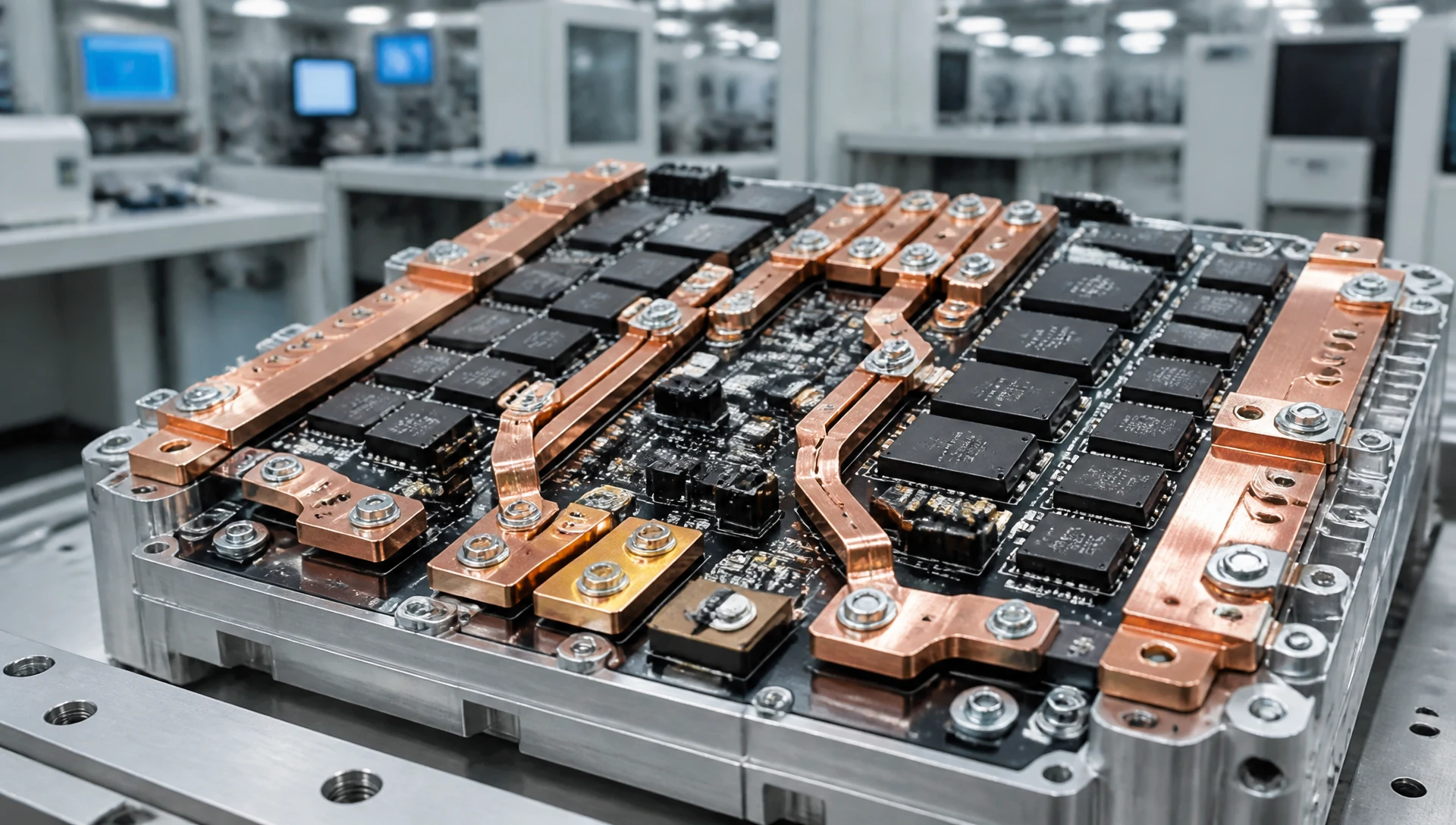
Designing a high-yield, heavy copper pcb cost-effective layout requires strict adherence to specialized Design for Manufacturability (DFM) rules. Thick copper structures alter chemical etching dynamics, meaning standard manufacturing rules must be updated.
As chemical etchants dissolve copper vertically down toward the FR4 substrate, they also dissolve copper laterally underneath the photoresist layer. This undercutting effect creates a trapezoidal trace profile rather than a perfect rectangle.
To account for this natural undercut, fabrication engineers implement specific design rules:
Minimum Trace Clearance Spaces: As copper thickness scales up, the minimum space required between adjacent traces must widen proportionally. For a 6oz heavy copper pcb, designers should maintain a minimum trace spacing of 15 to 18 mils (0.38 - 0.45 mm).
Minimum Trace Widths: To avoid excessive necking or trace narrowing during etching, the original artwork trace widths must be compensated. For an 8oz heavy copper pcb, the baseline layout width should not drop below 18 mils.
Enclosing a thick copper conductor profile presents challenges for standard solder mask applications:
The sharp 90-degree vertical step from the top of an 8oz copper trace down to the bare FR4 base measures approximately 280 um. Standard single-pass liquid photoimageable (LPI) spray methods cannot provide sufficient edge protection across these high vertical steps.
Advanced production teams must utilize multi-stage screen-printing processes or specialized high-viscosity resin fills. This ensures uniform encapsulation along the trace edges, eliminating micro-voids and preventing dendritic growth or moisture ingress during field operation.
A common point of confusion for procurement managers is balancing upfront raw material cost with total lifecycle assembly expenses. While purchasing thick copper base panels requires a larger initial material investment than standard boards, an expert heavy copper pcb supplier looks at total cost optimization.
Traditionally, factories handling extreme currents combined standard 2oz PCBs with secondary copper busbars, which were manually bolted or soldered onto the board surface by production line technicians.
Transitioning to a dedicated custom heavy copper pcb structure simplifies this process:
Labor Reduction: The monolithic construction integrates high-current power pathways directly inside the printed board panel. This entirely eliminates the labor costs associated with manual busbar fabrication, bending, and installation.
Reliability Boost: Mechanical fasteners and manual solder joints represent potential points of failure under thermal stress and mechanical vibration. Eliminating these joints improves long-term reliability.
Spatial Consolidation: Integrating high-current circuits and signal pathways on the same board minimizes the total assembly footprint. This allows engineers to design smaller enclosure footprints.
To review our complete capabilities across diverse base materials, layer stackups, and customized surface plating processes, explore our technical capabilities portal at
Transitioning a thick copper project from prototyping into high-volume manufacturing requires precise process synchronization. A thick copper board acts as a significant thermal sink during assembly, meaning standard automated soldering profiles must be carefully managed.
Because heavy copper traces excel at drawing heat away from local areas, they can pull thermal energy away from component solder pads during automated reflow cycles. This can lead to cold solder joints or tombstoning defects on smaller components.
Selective Profile Adjustments: Production engineers must extend the pre-heat soak duration within the reflow oven. This ensures the entire thick copper structure reaches a uniform temperature before entering the liquidus zone.
Thermal Relief Pad Design: All ground and power plane connections to component pads should utilize cross-shaped thermal relief geometries rather than solid copper pours. This thermal necking restricts heat transfer out of the pad during assembly, ensuring clean solder joints.
To optimize the manufacturing process, factories frequently select a partner that can provide a complete heavy copper pcb assembly service. Managing fabrication, material validation, and SMT assembly under a single vendor framework ensures that thermal reflow profiles match the exact thermal mass of the custom board stackup.
Maximizing the performance of heavy copper systems requires deep manufacturing expertise. As a fully certified, high-capability heavy copper pcb supplier, ApolloPCB manages every step of the high-current substrate fabrication process.
Our advanced facility is equipped with automated horizontal electroplating lines, heavy differential chemical etching chambers, and high-tonnage vacuum lamination presses. This enables us to reliably process internal and external copper weights from 3oz up to 15oz, while maintaining tight tolerances on internal trace geometries and plated via walls.
We source certified, high-grade copper foils and specialized high-Tg resin systems. This ensures your power supply modules, automotive controls, and energy storage assemblies maintain high performance through demanding thermal cycles.
Ready to optimize your high-current design, reduce manual assembly steps, and secure stable production routing? Head to our dedicated
Most commercial manufacturing facilities support reliable, volume-level production of copper weights up to 10oz (350 um) on both external and internal layers. Specialized industrial applications can be customized with extreme copper thicknesses reaching up to 20oz (700 um), provided the trace layout spacings are adjusted to accommodate the chemical etching factor.
Integrating thick copper layers directly into the board structure replaces manual, secondary busbars with a single, monolithic substrate. This eliminates separate mechanical fasteners and manual solder joints, which are common failure points in high-vibration environments. It also automates the assembly process, lowering labor overhead and reducing the risk of human error.
Thick copper boards require extended plating cycles in the electroplating baths. When exterior layers use a 6oz or 8oz copper profile, the factory adjusts processing times to ensure the inner barrels of plated through-holes (PTH) receive thick copper deposition (75 to 100 um). This heavy wall plating provides excellent current paths between layers and reinforces the via against thermal stress.

Got project ready to assembly? Contact us: info@apollopcb.com



 Whatsapp 0086 755 29438407
 Mail info@apollopcb.com
 Tel 0086 755 29438407


ABOUT US

PRODUCTS
TECHNOLOGY
KNOWLEDGE CENTRE
CULTURE
NEWS
We're not around but we still want to hear from you! Leave us a note:

Leave Message to APOLLOPCB
