




-
- PCB TYPE
- PRINTED CIRCUIT BOARD PROTOTYPE ALUMINUM PRINTED CIRCUIT BOARD R&F PCB FPC HIGH FREQUENCY PCB HIGH-TG PCB HEAVY COPPER PCB HDI PCB PCB FOR LIGHTING METAL CORE PCB


time:Jul 07. 2026, 20:14:56
The global electronics market is undergoing an era of rapid technological convergence, characterized by soaring current densities, hyperscale data transmission frequencies, and severe space constraints. As original equipment manufacturers (OEMs), automotive hardware engineers, and aerospace system architects design next-generation equipment—such as autonomous driving sensors, high-power industrial grid inverters, medical imaging systems, and advanced telecommunication infrastructure—the underlying printed circuit board ceases to be a simple passive component carrier. Instead, it serves as a highly critical, multi-dimensional electrical, thermal, and mechanical environment where even a microscopic material flaw or trace impedance deviation will trigger catastrophic field failures, localized thermal bottlenecks, and system-wide downtime.
For international procurement executives and engineering directors, navigating the global electronic supply chain requires separating high-volume brokers from a certified, technically capable high quality pcb manufacturer. While a standard low-cost broker focuses solely on short-term panel yield margins, an authoritative, asset-heavy manufacturing facility invests in advanced material sciences, automated cleanroom infrastructure, and strict verification protocols to guarantee long-term field survivability. This comprehensive engineering guide delivers a data-driven analysis of modern substrate selection, fine-line fabrication tolerances, layer-stackup integration, and strict quality assurance metrics required to execute high-reliability hardware production runs.
The electrical and thermal reliability of a circuit board is fundamentally dictated by the physical and chemical thresholds of its core laminate layers. When high-power components or ultra-fast processing chips run continuously, they subject the underlying board to severe thermal stress. Standard FR4 fiberglass laminates with low glass transition temperatures (Tg) swell and expand aggressively along the Z-axis under these loads, causing stress on copper-plated via barrels and tearing fine traces. Selecting an appropriate substrate class is the first baseline check executed during professional design-for-manufacturability (DFM) reviews.
To ensure long-term physical and signal stability under demanding operational conditions, engineering cells evaluate three distinct classes of advanced board substrates:
For heavy-duty industrial controller networks, multi-layered power boards, and high-amperage automation modules, choosing a high-Tg FR4 substrate (typically exceeding 170°C to 180°C) is mandatory. High-Tg laminates are formulated with advanced epoxy resins cross-linked with specialized curing agents to significantly reduce their Coefficient of Thermal Expansion (CTE). This molecular rigidity ensures the panel retains its structural flatness and mechanical strength during high-temperature lead-free convection reflow cycles, preventing trace distortion, interlayer delamination, and barrel cracking in plated through-holes.
As communication links expand into millimeter-wave spectrums and radar sensing fields, traditional FR4 substrates become unusable due to severe signal absorption and dielectric loss. For these setups, a specialized high frequency pcb manufacturer utilizes advanced hydrocarbon or polytetrafluoroethylene (PTFE) laminates, such as Rogers or Taconic core systems. These premium materials feature an exceptionally low and stable Dielectric Constant (Dk) and Dissipation Factor (Df) across broad temperature variations. This electrical consistency ensures high-speed signal propagation speeds, minimizes insertion loss, and eliminates phase distortion in dense radar arrays and telecom transceiver modules.
High-power LED arrays, electric vehicle (EV) powertrain controllers, and dense industrial power conversion grids generate massive thermal energy densities that can rapidly exceed the heat capacity of glass-epoxy panels. To resolve these thermal bottlenecks, a premier sinkpad pcb manufacturer implements direct thermal path metal core architectures. Unlike standard insulated metal boards where a thin dielectric layer separates the component pad from the metal base, Sinkpad technology mounts the thermal pad of high-output transistors or LEDs directly onto a solid copper or aluminum backing plate. This direct metallic connection allows thermal energy to flow unhindered into external cooling systems, keeping semiconductor junction temperatures within safe limits and extending product operating life.
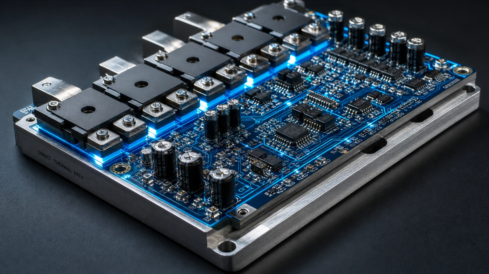
To guide your procurement cells and design teams during early schematic development, the technical matrix below cross-references the core mechanical, thermal, and electrical boundaries across different advanced substrate categories.
| Substrate Substrate Base Class | Thermal Conductivity (W/m-K) | Glass Transition Temp (Tg in °C) | Dielectric Constant (Dk at 1 GHz) | Dissipation Factor (Df at 1 GHz) | Z-Axis CTE (ppm/°C Pre-Tg) | Optimal Operational Sourcing Target |
| High-Tg FR4 (S1000-2 / IT180) | 0.35 to 0.45 | 175 to 185 | 4.3 to 4.6 | 0.015 to 0.020 | 45 to 50 | Multi-layer industrial controls, automotive mainboards |
| Rogers PTFE (RO4350B / RO4003C) | 0.62 to 0.69 | Greater than 280 | 3.48 to 3.55 | 0.002 to 0.003 | 30 to 32 | Automotive radar systems, high-speed telecom base stations |
| Direct Thermal Path Sinkpad Copper | 385 to 401 | N/A (Solid Metal) | N/A (Direct Pad) | N/A (Direct Pad) | 16 to 17 | High-output stadium LED arrays, EV powertrain converters |
Moving a multi-layer layout from initial CAD files into a reliable physical board requires state-of-the-art automated equipment and strict process controls. As traces and component spaces shrink to meet tight housing constraints, maintaining high yield rates requires high accuracy during chemical imaging, mechanical panel drilling, and multi-layer vacuum lamination. When looking to establish a secure procurement pipeline, sourcing managers often cross-reference global capabilities by researching
A fully integrated facility controls several critical processing phases to preserve mechanical and electrical tolerances:
Laser Direct Imaging (LDI) for Ultra-Fine Lines: Traditional factories utilize film photo-masks to transfer circuit patterns onto panels. However, these films are prone to minor stretching or dimensional shifting when exposed to cleanroom temperature changes, leading to pad misalignments. An advanced china pcb manufacturer avoids this risk by utilizing automated Laser Direct Imaging arrays. The LDI system scans the panel surface and uses a high-precision ultraviolet laser to trace the circuit layout directly onto the dry-film photoresist from digital files. This process automatically compensates for structural shifts across the panel, allowing factories to achieve fine-line trace widths and spaces down to 2.5 mils (63.5 microns) with high accuracy.
Controlled Multi-Zone Vacuum Lamination: Fabricating multi-layer panels requires stacking independent inner circuit layers with thin fiberglass prepreg sheets before sealing the layout under intense heat and pressure. The lamination press must maintain a highly accurate, multi-stage thermal profile alongside a constant vacuum seal. This tight control ensures the curing epoxy resin flows smoothly to fill all trace gaps without creating internal voids or micro-delaminations, which could trap moisture and cause early failure in the field.
Automated Mechanical and Laser Drilling Systems: Interlayer connections rely entirely on the quality of internal micro-vias and through-hole barrels. To maintain precise pad centers, high-speed CNC drilling systems utilize integrated vision-alignment cameras to verify panel dimensions before drilling. For fine-pitch blind and buried micro-vias, high-speed UV/CO2 laser drilling systems vaporize the dielectric resin with high accuracy, stopping exactly at the underlying target copper pad without damaging the inner-layer circuits.
Sourcing high-reliability electronics involves more than checking raw board parameters; it requires managing a unified assembly pipeline. When processing complex arrays or high-frequency modules, a purchasing team can reduce logistical risks and eliminate interface errors by selecting an integrated provider capable of handling raw board fabrication and surface-mount technology (SMT) component assembly under a single quality control workflow. Sourcing managers looking to streamline their initial prototyping pipelines can review our
Maintaining a defect-free automated assembly line requires strict process control across every production stage:
Inline 3D Solder Paste Inspection (SPI): More than 60% of all finished SMT defects originate from improper solder paste application. To address this risk, our high-speed printing cells pass every board through inline 3D SPI scanners immediately after paste deposition. These optical inspection systems measure paste height, volume, and alignment against target pad limits, catching paste printing variations before the board reaches component placement.
High-Speed Pick-and-Place Vision Systems: Modern SMT lines utilize high-speed component placers equipped with advanced optical vision systems. These systems verify the orientation and condition of every chip, diode, and fine-pitch Ball Grid Array (BGA) in real time, automatically correcting the mounting head's position down to the micron level before placing the component onto the solder paste.
Multi-Zone Convection Reflow Profiling: Lead-free solder alloys require precise control within multi-zone reflow ovens. The thermal profile must feature carefully managed preheating, soaking, liquidus reflow, and cooling stages. This precise control ensures all solder joints across varying component masses reach complete liquidation uniformly, preventing thermal shock, component shifting, or brittle joint structures. Enterprise buyers looking to transition complex designs into large-scale production can leverage the resources of our
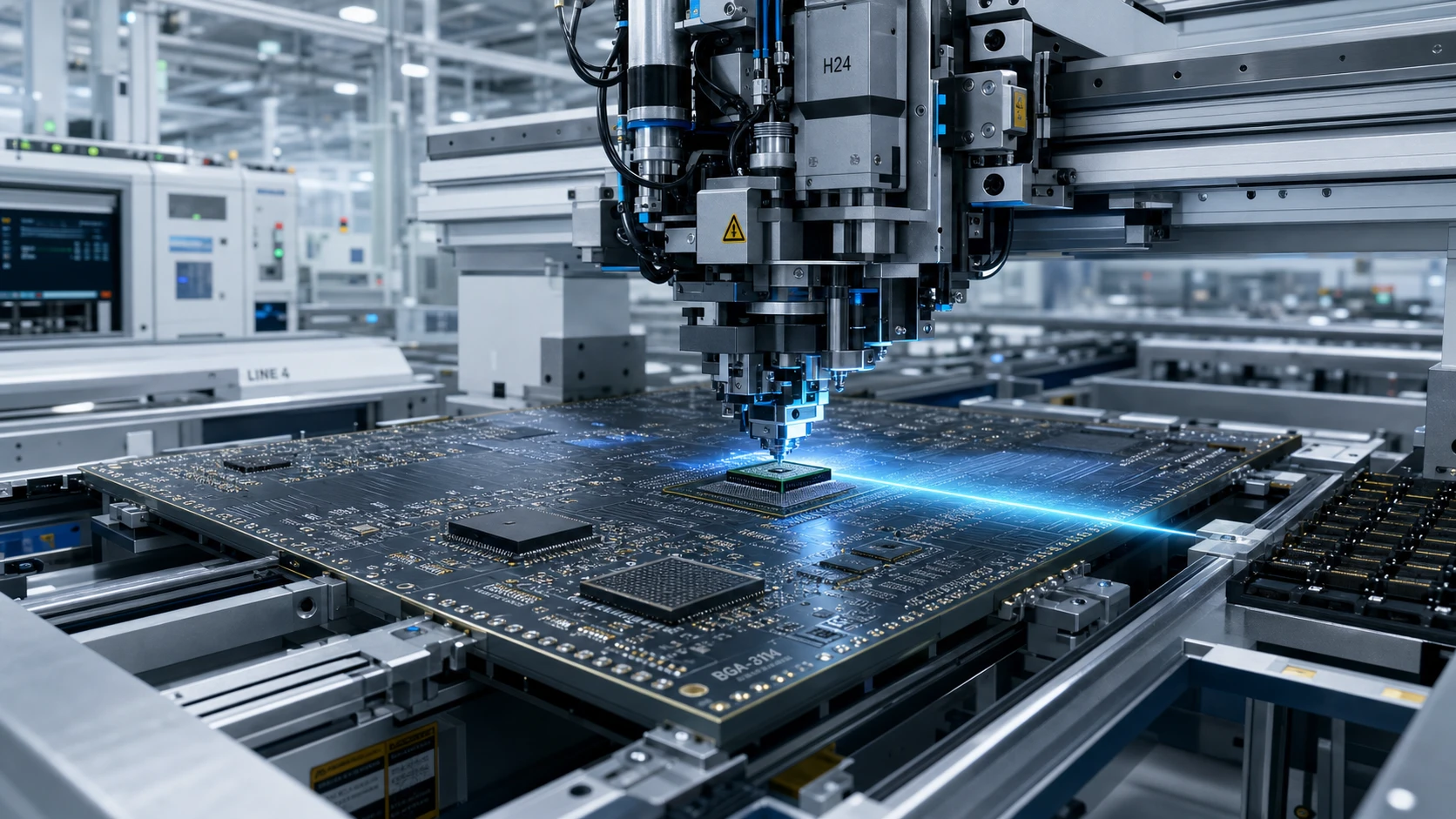
In demanding sectors like aerospace electronics, medical systems, and automotive safety modules, a single hidden manufacturing defect can cause major field liabilities and downtime. Therefore, premium pcb manufacturers in china must back all high-volume runs with verifiable data-driven testing protocols and strict quality management certifications.
Every high-reliability production run is processed under strict compliance with IPC Class 3 (Advanced High-Reliability Electronic Products) and IATF 16949 (Automotive Quality Management Systems) guidelines:
Automated X-Ray Inspection (AXI) for BGA Footprints: Components with bottom-side connections, such as fine-pitch BGAs and QFN packages, conceal their solder joints from standard optical cameras. To verify connection quality, completed boards pass through 3D automated X-ray scanners to check inside the solder layers, flagging internal voids, solder balls, or short circuits that optical inspection cannot see.
Destructive Metallographic Cross-Sectioning: To confirm long-term thermal via reliability, QA labs perform destructive cross-section analysis on sample coupons from each production batch. Technicians mount these test coupons in specialized resins, slice them open, and polish the cross-sections to inspect internal copper thickness under high-magnification microscopes. This step confirms the vertical copper plating inside the via barrels meets the mandatory thickness standards required to survive repetitive thermal expansion without fracturing.
100% Mandatory High-Potential (Hi-Pot) Insulation Testing: Completed assemblies undergo high-voltage insulation checks before final packaging. The automated test equipment applies a high-voltage pulse between separate circuit lines and adjacent ground planes to verify the integrity of the dielectric layers. This validation process ensures the board is free of pinholes, micro-cracks, or conductive chemical contamination that could cause low-voltage leakage currents or electrical shorts over long-term operation.

A qualified manufacturer operates an asset-heavy facility equipped with advanced Laser Direct Imaging (LDI) lines, inline 3D SPI/AOI testing systems, and automated multi-zone lamination presses to maintain tight process tolerances. In contrast, a low-cost broker lacks direct asset ownership and routinely subcontracts production runs to different factories, resulting in inconsistent material lots, wider dimensional tolerances, and higher field failure risks.
IPC Class 3 rules establish strict manufacturing thresholds for high-reliability electronic assemblies where continuous performance is mandatory and equipment downtime cannot be tolerated. This classification requires thicker vertical via barrel plating, tighter layer registration tolerances, and 100% non-destructive automated testing, ensuring the finished panels survive harsh vibration and thermal cycles in the field.
Your engineering team should switch to a Sinkpad configuration when your product layout features high-power components, such as high-output LEDs or power transistors, that generate intense localized heat density. Sinkpad technology removes the insulating dielectric layer directly beneath the component's thermal pad, creating a direct metallic path to the copper base plate that reduces thermal resistance and prevents premature component failure.
Succeeding in the highly competitive global electronics market requires moving past transactional brokers and partnering with an integrated manufacturer capable of executing advanced material science, complex chemical etching, and high-precision automated assembly under one roof. Maintaining a reliable product supply chain requires a manufacturing partner that combines deep technical expertise, advanced production machinery, and strict quality control frameworks.
ApolloPCB provides a vertically integrated manufacturing ecosystem equipped with advanced LDI imaging arrays, high-speed UV laser drilling cells, 3D automated optical inspection setups, and high-pressure vacuum lamination systems. Whether your design requires complex multi-layer configurations with dynamic flex specifications or specialized rigid-stiffener integration certified to IPC Class 3 standards, our engineering cells ensure your hardware scales smoothly with maximum reliability.
Ready to optimize your product sourcing pipeline, eliminate field failures, and streamline your volume production runs? Please contact our international support department and

Got project ready to assembly? Contact us: info@apollopcb.com



 Whatsapp 0086 755 29438407
 Mail info@apollopcb.com
 Tel 0086 755 29438407


ABOUT US

PRODUCTS
TECHNOLOGY
KNOWLEDGE CENTRE
CULTURE
NEWS
We're not around but we still want to hear from you! Leave us a note:

Leave Message to APOLLOPCB
