




-
- PCB TYPE
- PRINTED CIRCUIT BOARD PROTOTYPE ALUMINUM PRINTED CIRCUIT BOARD R&F PCB FPC HIGH FREQUENCY PCB HIGH-TG PCB HEAVY COPPER PCB HDI PCB PCB FOR LIGHTING METAL CORE PCB


time:Jul 23. 2026, 18:39:26
Global industrial equipment OEMs, medical device innovators, and automotive electronics engineers face a sharp increase in hardware complexity. As component footprints contract to 0201 passives and ultra-fine pitch Ball Grid Arrays (BGAs), achieving stable surface mount yields without thermal defects, tombstoning, or component bridging has become a major production bottleneck.
To protect time-to-market and field performance, international procurement managers rely on an expert smt assembly service. A certified assembly provider delivers more than just high-speed component placement. They provide end-to-end component sourcing verification, rigorous solder paste inspection, precise reflow thermal profiling, and comprehensive automated testing.
This technical guide offers a thorough engineering review of surface mount technology (SMT) workflows. We explore solder paste printing dynamics, automated component placement parameters, multi-zone reflow profiles, advanced inline inspection pipelines, and strategic supplier selection frameworks that help global factories achieve high production yields.
Executing high-yield circuit board assembly requires tight process control across every stage of the automated surface mount line. A leading smt assembly service manages each production variable to guarantee solder joint integrity and component alignment.
The solder paste printing phase accounts for nearly 60 to 70 percent of all SMT soldering defects. Applying an uneven solder paste volume leads to bridging on fine-pitch ICs or insufficient solder joints on passive components.
Laser-Cut Electro-Polished Stencils: High-capability factories use stainless steel stencils with smooth aperture walls to ensure complete paste release onto SMT pads.
3D Solder Paste Inspection (SPI): Immediately following the screen printer, automated 3D SPI systems measure the precise height, area, and volume of deposited paste. Any board showing aperture clogging or paste bridging is automatically flagged and cleaned before component placement.
Modern pick-and-place machinery combines high-speed chip shooters for passive components (0201, 0402) with high-precision multi-function heads for complex ICs, Quad Flat Packages (QFPs), and BGAs. Advanced vision alignment systems scan each component nozzle in real time, correcting X/Y offsets and rotational alignment down to sub-micron tolerances before placement.
The reflow soldering process transforms wet solder paste into strong, reliable intermetallic bonds. Achieving this requires precise multi-zone temperature control tailored to the specific thermal mass of the circuit board assembly.
Preheat Zone: Gradually ramps the board temperature at 1 to 3 degrees C per second to prevent thermal shock to delicate ceramic capacitors and base laminates.
Soak Zone: Maintains a steady temperature between 150 and 180 degrees C for 60 to 120 seconds. This activates the flux, removes volatile solvents, and balances temperatures across both light passives and heavy copper pours.
Reflow (Peaking) Zone: Raises the temperature above the liquidus point of lead-free solder (217 degrees C for SAC305) to a peak temperature of 240 to 250 degrees C. This forms clean, low-void solder fillets.
Controlled Cooling Zone: Rapidly cools the board at 3 to 6 degrees C per second. Controlled cooling refines the solder grain structure, enhancing mechanical strength and vibration resistance.
Tombstoning: Occurs when an uneven thermal mass or unequal solder paste volume causes one side of a passive component to wet faster than the other, pulling the component vertically. Balanced thermal relief pads and precise SPI checks eliminate this issue.
Solder Bridging: Caused by excessive paste deposition, component misalignment, or poor reflow profiles. Pre-reflow 3D AOI inspection catches misalignments before solder paste melts.
High-reliability electronics—such as industrial motor controllers, medical devices, and automotive modules—demand absolute zero-defect delivery. A certified smt assembly service incorporates multi-stage automated inspection throughout the production line.
Unlike older 2D systems that struggle with shadows and varying board heights, 3D AOI uses multi-angle projectors and high-resolution cameras to measure solder fillet volumes, component heights, and lead coplanarities. The system automatically detects missing components, polarity inversions, tombstoning, and insufficient solder joints.
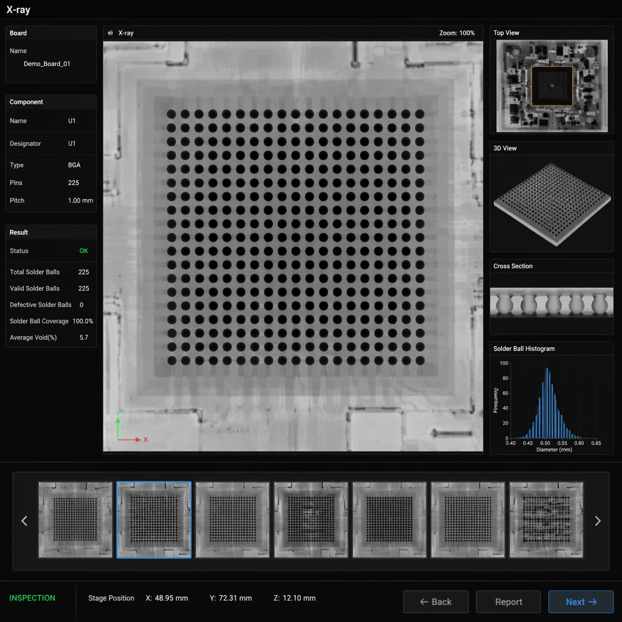
Modern IC packages hide their solder terminations directly beneath the silicon body. Standard optical cameras cannot verify solder joints under BGA, QFN, or Bottom Termination Components (BTC).
Automated 3D X-ray inspection penetrates these opaque packages to evaluate internal solder joint quality:
BGA Void Analysis: Measures internal void percentages within solder spheres, ensuring total void ratios stay well below the 15 to 25 percent IPC Class 2/3 limits.
Head-in-Pillow (HiP) Detection: Identifies incomplete solder coalescence caused by component warping during peak reflow temperatures.
Procurement executives frequently evaluate whether to invest in internal SMT placement lines or partner with a specialized contract assembly manufacturer. The table below outlines key operational parameters for factory teams.
| Operational Criteria | Internal SMT Line Setup | Professional SMT Assembly Service | Engineering Advantage for OEMs |
| Capital Investment (CAPEX) | High ($500K - $2M+ per line) | Zero direct equipment CAPEX | Reallocates corporate capital toward product R&D and market expansion. |
| Component Placement Speeds | Limited to owned line capacity | Scalable (50,000 to 200,000 CPH) | Effortlessly handles sudden demand spikes without production bottlenecks. |
| Advanced Inspection Tools | Often limited to manual/2D AOI | Full 3D SPI, 3D AOI, and 3D AXI | Guarantees IPC Class 3 quality standards for high-reliability applications. |
| Component Sourcing Reach | Relies on spot brokers | Global authorized distribution | Eliminates counterfeit component risks and lowers bill-of-materials (BOM) costs. |
| DFA Engineering Support | Limited internal review | Automated Design for Assembly | Catches layout errors early, preventing costly production line stops. |
To evaluate detailed technical parameters, surface mount tolerances, and high-speed feeder capacities, explore our specialized technical portal at
A high-yield assembly process depends heavily on authentic, high-quality electronic components. Inconsistent component packaging or counterfeit ICs can halt automated placement lines and degrade long-term field reliability.
                    TRACEABLE COMPONENT SOURCING FLOW
                                     │
   ┌─────────────────────────────────┼─────────────────────────────────┐
   ▼                                 ▼                                 ▼
[ Authorized Distribution ]   [ Incoming Verification ]   [ Climate-Controlled Storage ]
 - Direct factory ties         - Moisture sensitivity     - Nitrogen-purged cabinets
 - OCM lot traceability        - Counterfeit screening    - Bake-out ovens for MSL 3+
Authorized Sourcing Channels: Top-tier assembly facilities source components directly from Original Component Manufacturers (OCMs) or authorized distributors like Digi-Key, Mouser, and Arrow. This guarantees complete lot traceability and eliminates counterfeit risks.
Moisture Sensitivity Level (MSL) Controls: Plastic-encapsulated ICs absorb atmospheric moisture. If placed through reflow ovens without proper preparation, internal moisture expands rapidly, causing micro-cracking or "popcorning" defects. Professional SMT plants store MSL 3+ components in dry cabinets and bake them in climate-controlled ovens prior to assembly.
Partnering with an experienced assembly provider during the early design phase allows engineering teams to optimize board layouts for high-speed automated placement. Applying clear DFA principles ensures smooth volume production and lowers overall unit costs.
                 KEY DFA DESIGN CONSIDERATIONS FOR SMT

    Fiducial Marks                     Clearance Margins
    ┌───┐           ┌───┐              ┌──────────────────────────┐
    │ ⊙ │           │ ⊙ │              │ [Fine-Pitch BGA]         │
    └───┘           └───┘              │   ◄─── Minimum 3mm ───►  │
    Global Alignment Reference         │   Clearance to Edge      │
                                       └──────────────────────────┘
Global & Local Fiducial Placement: Place three global fiducial marks on panel corners for overall alignment, along with local fiducial pairs near fine-pitch ICs (under 0.5 mm pitch) and BGAs. This provides optical reference points for pick-and-place cameras.
Edge Clearance Margins: Maintain a minimum 3 mm to 5 mm unpopulated border along panel conveyor rails, or add break-away routing tabs to prevent placement nozzle collisions.
Standardized Component Orientation: Align polarized components (tantalum capacitors, diodes, IC Pin 1 marks) in the same direction across the panel. This simplifies visual inspection and speeds up automated programming.
Achieving high-yield SMT production requires an experienced manufacturing partner with deep process expertise. As a certified, high-capability smt assembly service provider, ApolloPCB handles every phase of the surface mount assembly workflow.
Our modern facilities feature high-speed automated placement lines, 3D SPI platforms, multi-zone nitrogen reflow ovens, 3D AOI scanners, and 3D X-ray inspection systems. This advanced infrastructure allows us to process complex boards—from quick-turn prototypes to high-volume IPC Class 3 builds—while maintaining tight quality control.
We enforce strict component traceability, maintain climate-controlled MSL storage, and provide thorough DFA reviews to ensure your industrial controls, medical devices, and automotive modules deliver reliable field performance.
Ready to improve your assembly yields, eliminate supply chain delays, and streamline volume manufacturing? Visit our
Because BGA solder connections are hidden beneath the component body, quality teams use automated 3D X-ray inspection (AXI) systems. 3D X-ray scans evaluate solder sphere shapes, detect bridging between adjacent pads, and measure internal void ratios to ensure compliance with IPC Class 2 and Class 3 standards.
3D Solder Paste Inspection occurs immediately after the solder paste printing phase. It measures the volume, height, and alignment of applied paste before component placement. Catching paste anomalies early prevents up to 70 percent of common reflow soldering defects, such as tombstoning, insufficient solder joints, and bridging.
A pre-production DFA review analyzes component spacings, fiducial mark placements, edge clearances, and pad geometries against automated line parameters. Resolving layout discrepancies early eliminates placement head collisions, improves soldering yields, and avoids costly line stops during volume production.

Got project ready to assembly? Contact us: info@apollopcb.com



 Whatsapp 0086 755 29438407
 Mail info@apollopcb.com
 Tel 0086 755 29438407


ABOUT US

PRODUCTS
TECHNOLOGY
KNOWLEDGE CENTRE
CULTURE
NEWS
We're not around but we still want to hear from you! Leave us a note:

Leave Message to APOLLOPCB
