




-
- PCB TYPE
- PRINTED CIRCUIT BOARD PROTOTYPE ALUMINUM PRINTED CIRCUIT BOARD R&F PCB FPC HIGH FREQUENCY PCB HIGH-TG PCB HEAVY COPPER PCB HDI PCB PCB FOR LIGHTING METAL CORE PCB


time:Jul 28. 2026, 10:01:24
International electronics manufacturing services (EMS) providers, automotive hardware engineers, and industrial equipment OEMs face an increasingly volatile hardware landscape. Navigating raw material price spikes, changing environmental compliance regulations, and rapid shifts toward High-Density Interconnect (HDI) structures requires accurate market intelligence.
Staying ahead of breaking pcb industry news is no longer just about monitoring sector trends. It is an essential risk management strategy for procurement officers, supply chain directors, and chief technology officers (CTOs). Timely technical insights allow manufacturing operations to hedge material costs, adjust stackup designs for global compliance, and secure reliable production capacity before shortages affect project timelines.
This comprehensive report examines key market developments shaping global printed circuit board fabrication. We review high-frequency laminate supply dynamics, AI-driven automation in smart factories, advanced substrate innovations, environmental compliance policies, and strategic sourcing models that ensure supply chain resilience.
Fluctuations in core raw material prices remain a top operational risk across global electronics manufacturing. Copper foil, epoxy resin, and glass fiber yarn represent the foundational costs of rigid and flexible laminates. Changes in these primary markets directly impact finished circuit board pricing.
Recent market reports indicate steady upward pressure on electrolytic copper foil prices, driven by high demand from electric vehicle (EV) battery manufacturing and global grid upgrades. At the same time, demand for high-temperature glass transition (High-Tg $\ge 170^\circ\text{C}$) resins continues to climb as industrial and automotive applications require better thermal endurance.
As processing speeds move past 112 Gbps PAM4 per channel, standard FR-4 laminates introduce severe signal attenuation and dielectric losses ($D_f$). Recent market coverage highlights a clear transition toward advanced laminate systems:
PTFE & Ceramic-Filled Substrates: Essential for 77 GHz automotive radar systems and satellite communication arrays, offering extremely low dissipation factors.
Ultra-Low Profile (ULP) Copper Foils: Reduces conductor skin effect losses at high frequencies, ensuring signal integrity in AI accelerator cards and high-speed enterprise servers.
The demand for smaller, more powerful hardware in medical devices, wearables, and aerospace avionics is driving rapid adoption of High-Density Interconnect (HDI) and Substrate-Like PCB (SLP) architectures.
To push trace width and spacing below 30/30 $\mu\text{m}$, tier-one fabricators are shifting from traditional subtractive etching to mSAP technology. Subtractive etching can cause trapezoidal trace profiles and undercutting on fine-pitch designs. By contrast, mSAP uses a thin seed copper layer and precise electroplating to build straight-walled copper traces, enabling high component density and controlled impedance.
Complex multi-layer HDI designs now routinely feature Any-Layer microvia structures, where laser-drilled copper-filled microvias directly connect any layer within the stackup. This eliminates deep buried vias, reduces board thickness by up to 40 percent, and shortens signal path lengths for high-speed processors.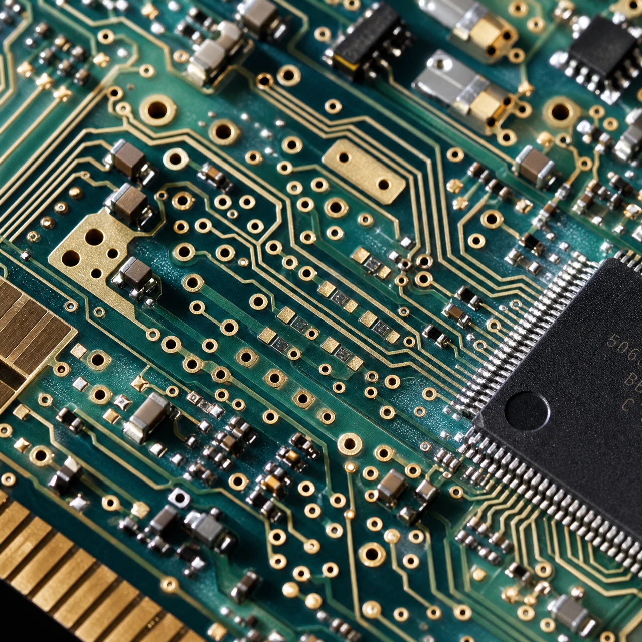
The implementation of Industry 4.0 principles is reshaping modern PCB manufacturing facilities. High-capability fabricators are integrating automated material handling systems, artificial intelligence (AI), and real-time sensor networks to improve production yields and operational transparency.
Traditional optical inspection engines rely on static rule sets, which often flag false positives due to normal copper reflectivity or minor laminate color variations. AI-driven AOI platforms use deep-learning models trained on millions of defect images:
False Alarm Reduction: AI filters out non-critical visual anomalies, allowing quality engineers to focus exclusively on real functional defects like hairline shorts, nicks, and copper slivers.
Predictive Process Tuning: Defect pattern analysis automatically alerts etch line operators when chemical concentrations drift, preventing volume yield drops before they happen.
Advanced plating lines now use online titrators and closed-loop sensors to maintain copper sulfate, acid concentrations, and organic additives at precise levels. This continuous monitoring ensures uniform copper plating thickness across high-aspect-ratio microvias and deep blind holes.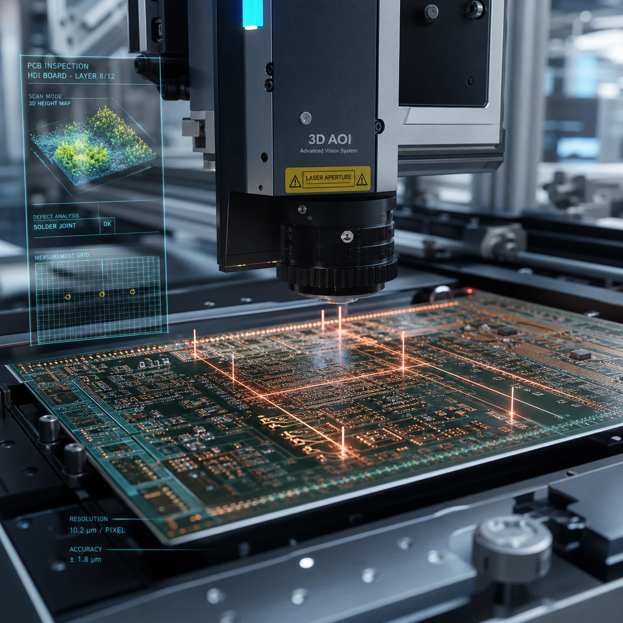
To help purchasing managers evaluate vendor capabilities, the table below compares traditional board fabrication approaches with advanced smart factory processes.
| Operational Criteria | Traditional Board Fabrication | Next-Gen Smart PCB Manufacturing | Engineering Advantage for OEMs |
| Trace Width & Spacing Limits | 75/75 um (Subtractive Etch) | < 25/25um (mSAP / SAP) | Supports ultra-fine pitch BGAs and micro-SoCs without routing bottlenecks. |
| Microvia Registration Accuracy | ± 38um (Mechanical alignment) | ±12um(Laser CCD alignment) | Prevents annular ring breakout on dense multi-layer HDI stackups. |
| Inspection & Quality Control | Manual visual + 2D AOI | AI 3D AOI + Inline 3D AXI | Eliminates human oversight error; guarantees IPC Class 3 compliance. |
| Supply Chain Traceability | Batch-level paper logs | Unique QR code per board / MES tracking | Provides complete material, operator, and process parameter history for audits. |
| Thermal Testing Capabilities | Basic thermal stress bake | Real-time IST & IST-like testing | Verifies long-term barrel reliability for automotive and aerospace hardware. |
To stay informed on market developments, technological breakthroughs, and industry analysis, explore our dedicated news hubs at
Environmental regulations continue to reshape manufacturing protocols across the electronics industry. Global OEMs must ensure that every circuit board component and substrate complies with evolving international directives.
To comply with strict green building standards and regional electronic waste directives, industrial OEMs are shifting toward halogen-free materials. Replacing bromine-based flame retardants with phosphorus- or nitrogen-based compounds reduces toxic gas emission risks during end-of-life recycling without compromising thermal performance or flammability ratings (UL 94V-0).
Leading PCB fabricators are investing heavily in zero-liquid-discharge (ZLD) infrastructure:
Copper Metal Recovery: Electrolytic recovery units extract pure metallic copper directly from spent micro-etching solutions, reducing hazardous waste generation by up to 80 percent.
Process Water Recycling: Closed-loop filtration and reverse-osmosis systems allow factories to recycle more than 75 percent of rinsing water back into production lines.
Recent global logistics disruptions have underscored the risks of single-source procurement strategies. Leading OEMs are diversifying their supply chains to ensure production continuity and maintain cost stability.
Dual-Tooling and Parallel Prototyping: Validating Gerber files and panel layout designs across primary and secondary manufacturing sites ensures smooth volume migration if a regional facility experiences downtime.
Vendor-Managed Inventory (VMI): Establishing VMI programs for critical laminates, specialized solder masks, and rare IC packages buffers against sudden material lead-time spikes.
Comprehensive DFM Audits: Running automated Design for Manufacturability reviews before releasing production orders ensures stackups utilize widely available core and prepreg thicknesses, avoiding custom material delays.
Adapting to technical advancements and market shifts requires a knowledgeable, agile manufacturing partner. As a certified leader in advanced PCB fabrication and turnkey assembly, ApolloPCB translates market trends into practical manufacturing solutions.
Our modern facilities feature high-precision laser direct imaging (LDI), multi-layer optical registration alignment, automated mSAP etching lines, and 3D AOI inspection systems. Whether you are producing high-frequency 5G communications equipment, automotive power electronics, or high-density industrial control panels, ApolloPCB delivers consistent quality, full material traceability, and IPC Class 3 precision.
By maintaining direct relationships with global laminate manufacturers and enforcing rigorous internal quality controls, we protect your hardware projects from material supply disruptions and unexpected cost fluctuations.
Stay competitive with reliable market intelligence and professional board fabrication capabilities. Visit our
ApolloPCB maintains direct strategic partnerships with major global laminate suppliers (such as Shengyi, Isola, Rogers, and Taconic). Our procurement teams track raw material price indices and lead-time developments continuously, allowing us to pre-stock high-demand cores and prepregs to protect customer project schedules.
Modified Semi-Additive Process (mSAP) technology allows fabricators to achieve trace widths and spacings below $30\ \mu\text{m}$ with straight copper sidewalls. This satisfies the demand for extreme miniaturization in high-density electronics, outperforming traditional subtractive etching methods in both circuit density and signal integrity.
ApolloPCB strictly adheres to RoHS 3, REACH, and ISO 14001 standards. We offer a broad range of halogen-free laminates, lead-free surface finishes (such as ENIG, Immersion Silver, and Lead-Free HASL), and operate zero-discharge water recycling systems to help OEM partners fulfill global corporate sustainability goals.

Got project ready to assembly? Contact us: info@apollopcb.com



 Whatsapp 0086 755 29438407
 Mail info@apollopcb.com
 Tel 0086 755 29438407


ABOUT US

PRODUCTS
TECHNOLOGY
KNOWLEDGE CENTRE
CULTURE
NEWS
We're not around but we still want to hear from you! Leave us a note:

Leave Message to APOLLOPCB
