




-
- PCB TYPE
- PRINTED CIRCUIT BOARD PROTOTYPE ALUMINUM PRINTED CIRCUIT BOARD R&F PCB FPC HIGH FREQUENCY PCB HIGH-TG PCB HEAVY COPPER PCB HDI PCB PCB FOR LIGHTING METAL CORE PCB


time:Jul 10. 2026, 13:57:25
The global electronics industry is moving toward relentless miniaturization, lower weight profiles, and dynamic mechanical flexibility. For original equipment manufacturers (OEMs), automotive hardware innovators, and advanced industrial medical factories, securing an agile partner for custom fpc fabrication is no longer just a supply chain checkbox—it is a critical architectural pillar. Flexible Printed Circuits (FPCs) demand a manufacturing precision that far exceeds standard rigid board production due to the unique behavior of flexible polyimide substrates under thermal and mechanical stress.
This comprehensive factory-level guide breaks down the micro-engineering behind the high precision fpc fabrication process, addresses common engineering pain points, and outlines the structural quality frameworks necessary to move your custom flexible circuit from high-fidelity prototype to global market distribution.
A high-performance flexible circuit is entirely dependent on the structural integrity of its core laminates. Unlike rigid PCBs that rely on woven fiberglass composites (FR-4), standard custom fpc fabrication utilizes specialized engineering polymers engineered to withstand thousands of continuous dynamic bending cycles without electrical trace degradation.
1.1 Base Films: Polyimide (PI) vs. Polyester (PET)
Polyimide (PI): The absolute gold standard for industrial, aerospace, and medical factory applications. Polyimide exhibits exceptional thermal stability (withstanding lead-free SMT reflow temperatures exceeding 260°C), superior dielectric strength, and unmatched flexibility.
Polyester (PET): Primarily restricted to low-cost, low-temperature consumer applications like membrane switches. PET cannot survive automated SMT reflow profiles, making it unsuitable for advanced factory-level integration.
The choice of copper foil defines the mechanical lifespan of your flexible circuit:
Electro-Deposited (ED) Copper: Possesses a vertical grain structure. It is highly economical and perfectly suited for static flexible applications where the board only needs to fold once during final product casing assembly.
Rolled Annealed (RA) Copper: Undergoes heavy mechanical compression to create an elongated horizontal grain layout. RA copper is mandatory for dynamic flex applications (such as hinges, robotic joints, or optical disk drive pickups) where the circuit faces constant movement. Failing to specify RA copper in dynamic applications is a primary cause of early field failures due to micro-cracking.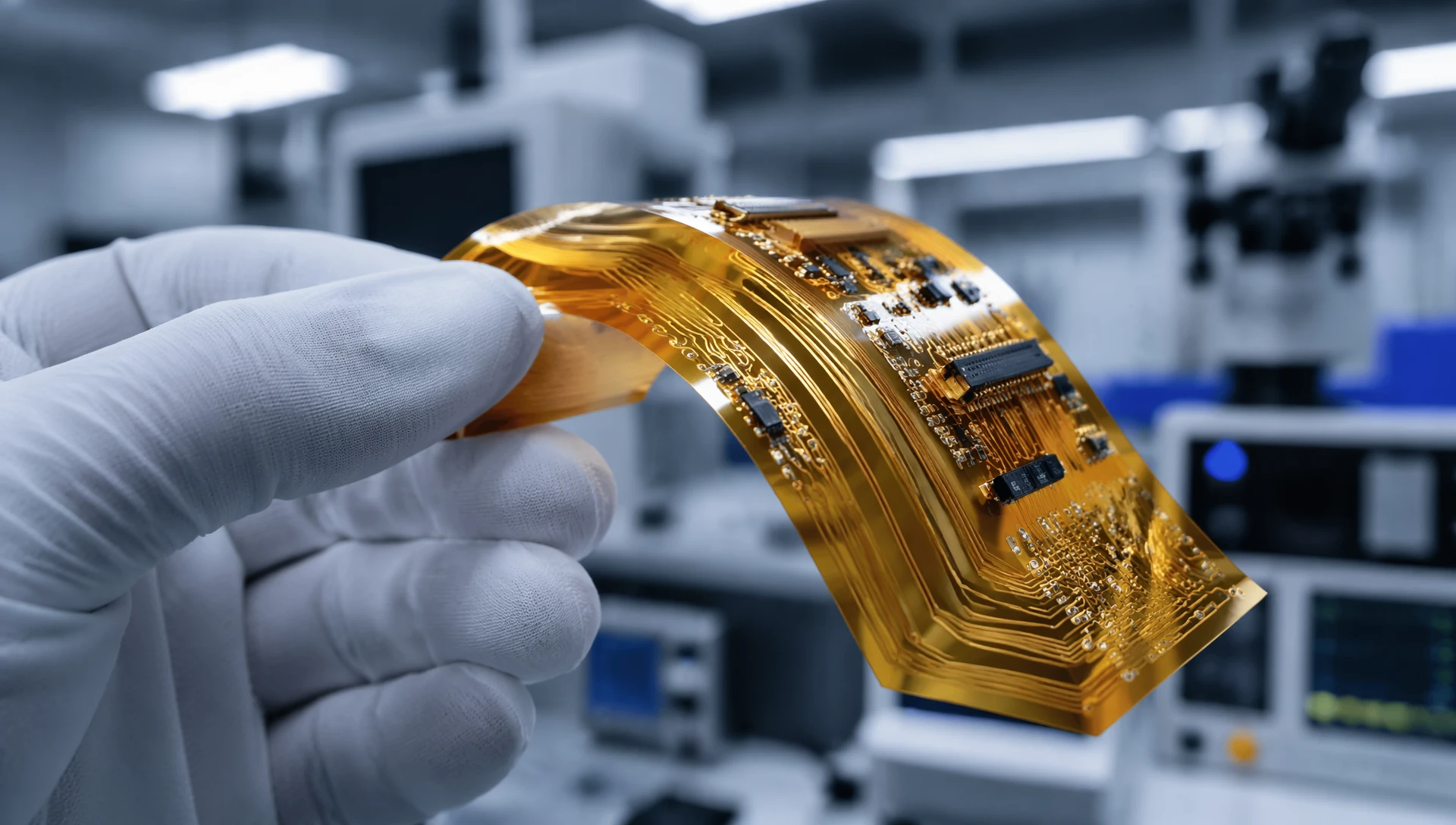
To achieve the sub-mil registration tolerances required by modern high-density interconnect (HDI) designs, a manufacturer must abandon manual registration methodologies. Achieving top-tier quality requires an investment in advanced hardware systems and automated optical alignment across every segment of the production line. For a closer look at these dedicated technical parameters, you can review our technical documentation covering the specialized
Traditional photo-tooling utilizes glass or film masks that expand and contract under cleanroom temperature shifts, introducing subtle layer-to-layer misalignments. A premium high precision fpc fabrication process relies on Laser Direct Imaging (LDI).
LDI systems beam the CAD circuit pattern directly onto the photoresist-coated polyimide film via computer control. This eliminates film distortion entirely, enabling the stable production of ultra-fine trace widths and spaces down to 2 mils (0.05mm) or less. This level of trace density is a critical requirement for factories manufacturing modern high-resolution display interfaces and medical sensor arrays.
Once the pattern is imaged, the exposed copper must be chemically etched with absolute uniformity. Uncontrolled chemical pooling can lead to over-etching or under-etching, which significantly alters trace impedance profiles.
Furthermore, during the mechanical or UV laser drilling of micro-vias, friction melts the internal resin, creating "drill smear" over the copper interconnect pads. High-end custom fabrication utilizes advanced plasma desmear chambers, where an ionized gas mixture strips away organic residues at a molecular level, guaranteeing perfect electrical continuity across multi-layer flexible stack-ups.
While single and double-sided flexible circuits handle a large percentage of routing tasks, advanced industrial electronics often require complex multilayer architectures to manage high signal counts, dense ground shielding planes, and controlled impedance requirements. To explore how our manufacturing plant structures these complex stack-ups, you can inspect our main capability overview on the
As layer counts scale to 4, 6, or 8 layers, the main challenge during the high precision fpc fabrication process centers on Z-axis expansion and structural rigidity. Since multiple layers of polyimide and adhesive restrict natural flexing, engineers must design specialized "air-gap" or unbonded layer configurations. In an air-gap configuration, individual flexible layers are left unbonded in areas that undergo severe bending, allowing them to slide independently and dramatically reducing internal mechanical tension.
For absolute optimization in tight spatial environments, engineering teams frequently cross-pollenate technologies to eliminate connectors and cables entirely. For high-reliability environments, scaling up your design to combine standard FR-4 materials with internal polyimide layers offers maximum structural durability. To evaluate the mechanical integration parameters of these complex designs, hardware teams can read our production guidelines on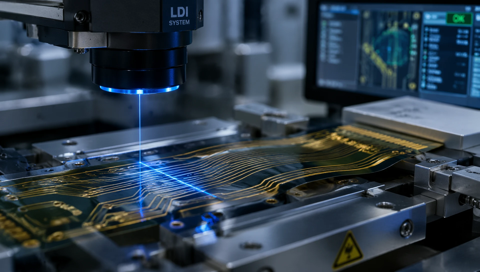
Design for Manufacturing (DFM) for flexible circuitry follows a completely different set of structural laws compared to rigid board design. Applying rigid design rules to an FPC layout will inevitably result in physical tearing, trace delamination, and expensive manufacturing delays.
Copper traces on a flexible substrate act like structural beams under mechanical tension. Sharp 90-degree or 45-degree trace turns create severe mechanical stress accumulation points. Under continuous bending, these locations will develop micro-fractures.
Solution: All trace transitions inside a bend zone must feature curved, radiused corners.
Avoiding the I-Beam Effect: If your design features a two-layer flex layout, running a top-layer trace directly over a bottom-layer trace creates an "I-Beam" structure. This drastically increases the stiffness of the circuit and leads to rapid metal fatigue. Traces on the top and bottom layers must be staggered or alternated to spread out physical compression evenly across layers.
Flexible copper pads are highly susceptible to lifting off the polyimide base film during component soldering or physical bending due to the smooth surface profile of the substrate.
Tie-Downs / Anchor Pads: Every surface-mount or through-hole pad must feature extended copper "ears" or anchors that extend beneath the insulating coverlay material to mechanically lock the pad in position.
Coverlay Over Solder Mask: Standard liquid photoimageable (LPI) solder mask is brittle and will crack immediately when bent. A professional custom fpc fabrication house utilizes solid Polyimide Coverlays laminated under high heat and vacuum pressure. The coverlay openings are pre-cut via CNC lasers or precision dies to ensure accurate exposure of component landing zones while providing full encapsulation for the rest of the circuit.
While FPCs are designed to bend, the specific locations where components (such as microcontrollers, connectors, and passives) are soldered must remain completely rigid. Placing components on a flexible section will cause solder joints to fracture or components to pop off during mechanical movement.
To create localized rigidity, specialized backing materials are selectively laminated to the reverse side of the FPC using high-strength thermo-setting adhesives or pressure-sensitive tape (like 3M 467MP):
FR-4 Stiffeners: Woven fiberglass blanks laminated beneath SMT connector footprints to mimic standard rigid board handling characteristics during automated pick-and-place processing.
Polyimide (PI) Stiffeners: Extra layers of thick polyimide film applied to increase the overall local thickness of the board. These are commonly used on the insertion tips of Zero Insertion Force (ZIF) connectors to meet strict plug-in thickness tolerances (typically 0.3mm).
Aluminum/Stainless Steel Stiffeners: Deployed in ultra-compact designs that demand high structural rigidity combined with heat dissipation capabilities, such as high-power LED driver arrays or automotive sensors.
Partnering with an inexperienced manufacturer for flexible circuits can result in catastrophic field failures due to micro-voids, poor layer registration, or substandard raw materials. Sourcing managers must evaluate a custom fpc fabrication supplier using a transparent technical assessment framework. To analyze our exact manufacturing process and view our inventory of specialized base laminates, feel free to explore our primary capability node on our
A world-class B2B manufacturing plant must enforce rigorous testing to validate the reliability of flexible circuit runs:
Controlled Impedance Testing: Uses Time Domain Reflectometry (TDR) systems to verify that high-speed signal paths (e.g., USB 3.0, HDMI, MIPI) meet tight impedance tolerances.
Thermal Shock and Moisture Resistance Testing: Subjects production samples to extreme cyclic temperature variations (-40°C to +125°C) to verify that no layer separation or adhesive degradation occurs.
Flying Probe Electrical Testing: Verifies 100% electrical open-and-short circuit isolation across every trace path before shipping, ensuring hassle-free assembly on your SMT line.

A: While standard single and double-sided flexible circuits make up the majority of production runs, advanced facilities can achieve high-precision multilayer FPC fabrication up to 8 layers. At ApolloPCB, we employ specialized Laser Direct Imaging (LDI) and advanced vacuum lamination presses to handle complex multi-layer configurations while maintaining tight registration and impedance metrics.
A: Preventing trace failure requires a combination of strict design-for-manufacturability rules and premium raw materials. At ApolloPCB, our engineering team enforces the use of Rolled Annealed (RA) copper instead of Electro-Deposited (ED) foils for dynamic joints. We also optimize track paths to use radiused curves and staggered trace placement layouts to eliminate mechanical stress concentration points.
A: Traditional liquid photoimageable (LPI) solder mask is rigid and brittle, meaning it will crack and flake off under minimal mechanical bending. A polyimide coverlay is a solid engineering film laminated under high pressure, providing identical flexible performance to the base core material. ApolloPCB utilizes laser-cut coverlays to guarantee robust insulation and protect fine-pitch traces through thousands of operational bending cycles.
Navigating the engineering requirements of modern flexible circuitry demands more than just standard manufacturing execution—it requires proactive co-engineering. By understanding how core substrate chemistry, automated imaging tolerances, and optimized layout design rules interact, your sourcing organization can prevent engineering delays, eliminate hidden rework costs, and build a highly dependable product.
ApolloPCB is an industry-leading, ISO 9001:2015 and IATF 16949 certified electronics manufacturer specializing in advanced custom fpc fabrication and turnkey printed circuit solutions. From high-speed, quick-turn engineering prototypes to full-scale automated factory production runs, our dedicated hardware engineering team provides comprehensive design-for-manufacturability reviews to optimize your design, protect your engineering budgets, and ensure absolute long-term reliability in the field.
Ready to eliminate supply chain delays and experience the precision of world-class flexible electronics manufacturing? Contact our global engineering support desk today to receive an itemized, clear technical quotation tailored to your exact custom specifications.

Got project ready to assembly? Contact us: info@apollopcb.com



 Whatsapp 0086 755 29438407
 Mail info@apollopcb.com
 Tel 0086 755 29438407


ABOUT US

PRODUCTS
TECHNOLOGY
KNOWLEDGE CENTRE
CULTURE
NEWS
We're not around but we still want to hear from you! Leave us a note:

Leave Message to APOLLOPCB
