




-
- PCB TYPE
- PRINTED CIRCUIT BOARD PROTOTYPE ALUMINUM PRINTED CIRCUIT BOARD R&F PCB FPC HIGH FREQUENCY PCB HIGH-TG PCB HEAVY COPPER PCB HDI PCB PCB FOR LIGHTING METAL CORE PCB


time:Jul 31. 2026, 14:56:01
Industrial automation engineers, medical instrument designers, and automotive electronics OEMs face unprecedented performance demands. As hardware designs incorporate high-density multi-layer stackups, ultra-fine pitch Ball Grid Arrays (BGAs), and high-power thermal management structures, ensuring seamless alignment between board fabrication and component placement has become a critical operational priority.
To eliminate component mismatch risks, reduce expensive engineering revisions, and shorten time-to-market, procurement directors increasingly rely on integrated pcb manufacturing and assembly services. A single-source EMS partner manages the entire production cycle—from raw laminate sourcing and copper etching to surface mount placement, automated optical testing, and functional verification.
This comprehensive engineering guide reviews every phase of high-reliability circuit board production. We analyze multi-layer panel fabrication, surface mount technology (SMT) workflows, advanced inspection protocols, and strategic supplier selection frameworks that help global factories maximize manufacturing yields.
Executing high-reliability hardware production requires precise synchronization between raw board fabrication and final SMT line setups. Fragmented manufacturing—where fabrication occurs at one facility and component mounting at another—frequently introduces alignment delays, component pad mismatches, and disputed defect liability.
Selecting an integrated turnkey pcb manufacturing and assembly workflow eliminates operational friction and protects engineering intent throughout the production cycle:
Unified DFM and DFA Analysis: Running simultaneous Design for Manufacturability (DFM) and Design for Assembly (DFA) reviews ensures panel margins, fiducial placements, solder mask clearances, and component pads are fully optimized before tooling begins.
Single-Point Quality Accountability: Integrating fabrication and assembly under one quality management system eliminates vendor finger-pointing if solderability issues, trace delamination, or component pad dewetting occur.
Optimized Supply Chain Timelines: Consolidating fabrication lead times, component procurement, and line scheduling reduces total turnaround times by up to 30 to 40 percent compared to split-vendor models.
Industrial equipment controls operate in harsh thermal, mechanical, and electrical environments. Achieving long-term field stability begins with high-grade laminate materials, controlled impedance trace routing, and robust surface finishes.
High-Tg FR-4 Laminates: Industrial control boards exposed to continuous operating temperatures require glass transition temperatures (Tg >= 170°C) and high decomposition temperatures (Td >= 340°C) to prevent z-axis expansion and barrel cracking during thermal cycling.
Controlled Impedance Execution: High-speed communication interfaces (PCIe, USB 3.2, Gigabit Ethernet) rely on tight trace width and dielectric distance controls. Fabricators utilize specialized field solvers to maintain impedance tolerances within ±5% to ±10%.
Choosing an appropriate surface finish directly impacts component solderability, shelf life, and fine-pitch placement accuracy:
Electroless Nickel Immersion Gold (ENIG): Provides an exceptionally flat planar surface, making it ideal for fine-pitch BGAs, QFNs, and 0201 passives. Offers superior corrosion resistance and long shelf life.
Lead-Free HASL (Hot Air Solder Leveling): Cost-effective for standard through-hole and broad-pitch SMT designs, though less suited for ultra-fine pitch components due to uneven surface contours.
Organic Solderability Preservatives (OSP): Delivers a flat copper surface at a low cost, widely used in high-volume automotive and consumer assemblies requiring lead-free processing.
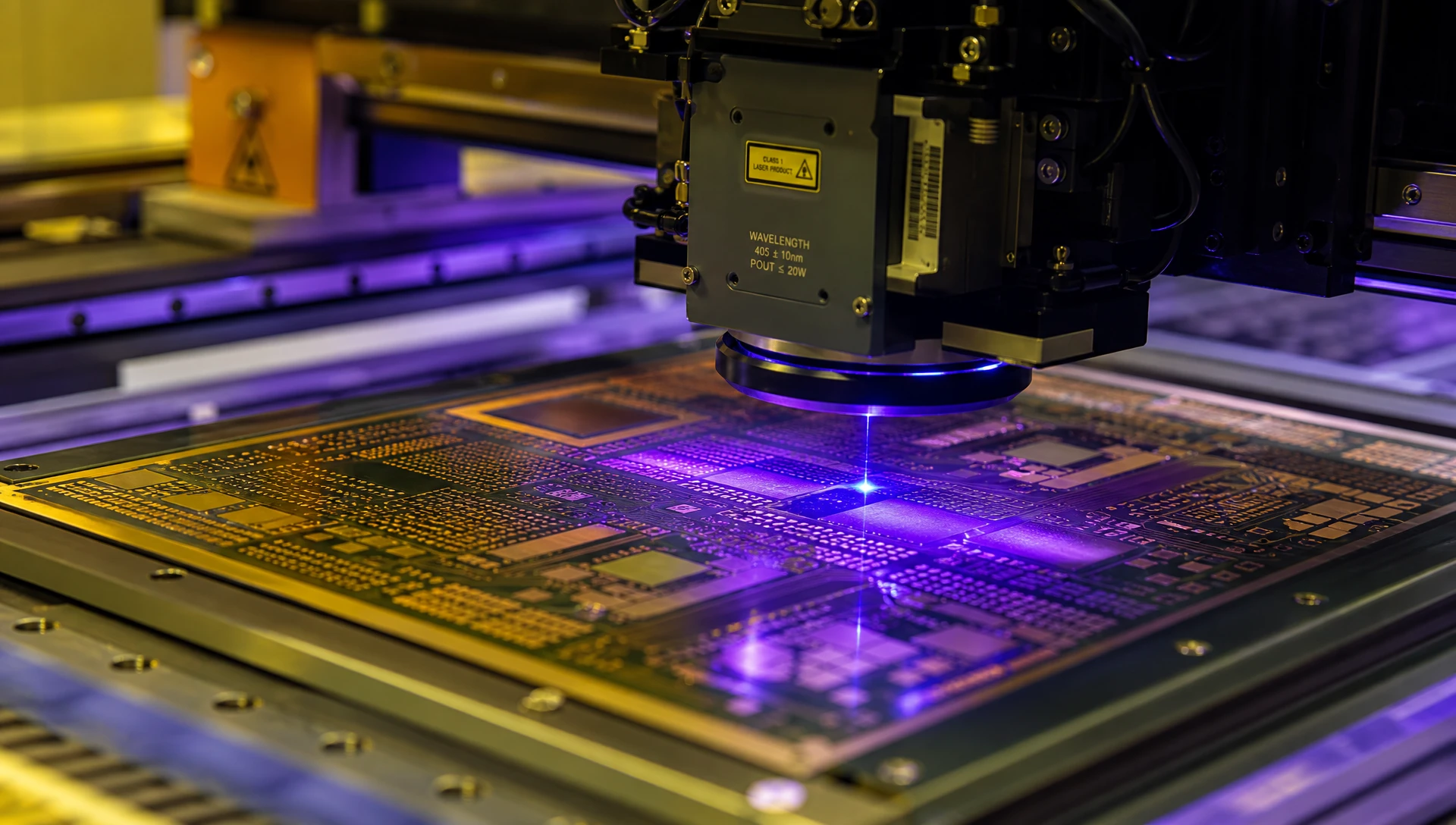
Once raw board panels pass electrical testing, automated surface mount technology (SMT) and through-hole technology (THT) lines populate the boards according to the customer's Bill of Materials (BOM).
Modern pick-and-place machinery combines high-speed chip shooters for passive components (0201, 0402) with high-precision multi-function vision heads for complex ICs, Quad Flat Packages (QFPs), and BGAs. Advanced optical alignment systems scan component leads and BGA solder spheres in real time, adjusting X/Y positional offsets and rotational alignment before placement.
For industrial pcb manufacturing and assembly projects incorporating heavy power connectors, transformers, and heat-sink mounted MOSFETs, automated selective wave soldering or pin-in-paste (PIP) reflow processes are applied. Selective wave soldering isolates specific through-hole leads, protecting nearby sensitive surface mount components from excessive thermal exposure.
High-reliability electronics—such as industrial motor drives, medical monitoring equipment, and energy management devices—demand zero-defect manufacturing standards. Leading assembly facilities incorporate multi-tier inspection throughout the production line.
3D Solder Paste Inspection (SPI): Measures precise solder paste volume, height, and coverage area immediately after stencil printing. Catching paste anomalies early eliminates nearly 70 percent of common reflow soldering defects.
3D Automated Optical Inspection (AOI): Uses multi-angle cameras and blue/red LED arrays to evaluate solder fillet shapes, component orientations, tombstoning, and pad bridging post-reflow.
3D Automated X-Ray Inspection (AXI): Inspects non-visible solder connections under BGA, QFN, and Bottom Termination Components (BTC). AXI systems verify solder ball wetting and ensure internal void ratios remain well below IPC Class 2/3 limits (<15% to 25%).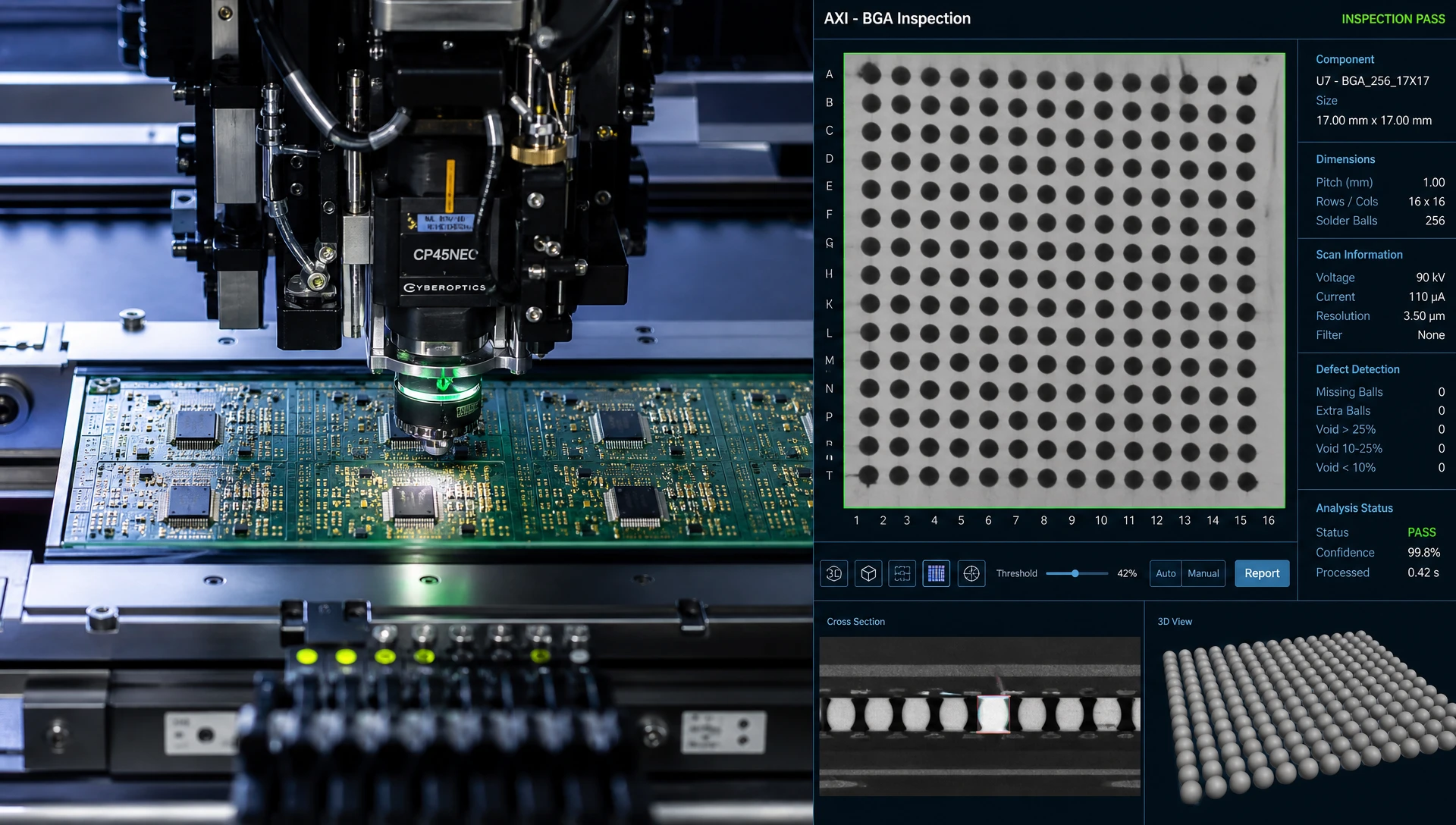
Manufacturing managers frequently assess whether to maintain internal assembly equipment or partner with a dedicated turnkey assembly facility. The comparison table below highlights key operational parameters.
| Performance Parameters | In-House Manufacturing Setup | Specialized Turnkey Assembly Partner | Engineering Advantage for Factory Clients |
| Capital Expenditure (CAPEX) | High ($1M - $3M+ per line setup) | Zero capital equipment outlay | Reallocates corporate capital toward product R&D and core market growth. |
| Placement Flexibility | Restricted to owned equipment limits | Scalable (0201 to fine-pitch BGA) | Handles rapid volume fluctuations without capacity bottlenecks. |
| Quality Inspection Tools | Often limited to 2D optical checks | Full 3D SPI, 3D AOI, and 3D AXI | Guarantees compliance with IPC Class 3 high-reliability standards. |
| Component Sourcing Reach | Dependent on localized brokers | Global authorized distribution network | Prevents counterfeit component risks and lowers overall BOM costs. |
| DFM/DFA Engineering | Limited internal review scope | Dedicated automated engineering review | Identifies design flaws early, preventing costly production delays. |
To review detailed cost structures, layer stackup options, and volume pricing factors, consult our comprehensive guide on
High-yield electronics assembly relies on authentic, high-quality electronic components. Inconsistent packaging, poor storage, or counterfeit ICs can stall automated placement lines and compromise long-term field reliability.
Authorized Distribution Networks: Tier-one facilities procure components directly from Original Component Manufacturers (OCMs) or franchised global distributors (e.g., Digi-Key, Mouser, Arrow). This guarantees complete lot traceability and protects projects from counterfeit components.
Moisture Sensitivity Level (MSL) Controls: Plastic-encapsulated ICs absorb atmospheric moisture. Uncontrolled exposure causes steam expansion during reflow, leading to internal micro-cracking ("popcorning"). Certified assembly plants store MSL 3+ components in nitrogen-purged dry cabinets and apply controlled bake-out cycles prior to placement.
Collaborating with an experienced manufacturing partner during the initial design phase allows hardware engineers to optimize board layouts for high-speed automated placement, ensuring smooth volume production and competitive unit costs.
Fiducial Mark Strategy: Place three global fiducial marks on panel corners for overall board alignment, alongside local fiducial pairs adjacent to fine-pitch BGAs (under 0.5 mm pitch). This provides optical reference points for pick-and-place cameras.
Panel Clearance Rails: Maintain a minimum 5 mm unpopulated border along panel conveyor rails, or add break-away routing tabs to prevent placement nozzle collisions.
Polarity Alignment: Orient polarized components (tantalum capacitors, diodes, IC Pin 1 indicators) in the same direction across the panel. This simplifies automated inspection and speeds up pick-and-place programming.
Achieving high-yield circuit board production requires a reliable, technology-driven manufacturing partner. As a certified leader in pcb manufacturing and assembly, ApolloPCB delivers end-to-end manufacturing solutions for factory clients worldwide.
Our modern manufacturing facility features high-precision laser direct imaging (LDI), multi-layer optical alignment systems, high-speed SMT placement lines, multi-zone nitrogen reflow ovens, 3D AOI inspection, and 3D X-ray (AXI) testing systems. From quick-turn prototypes to high-volume IPC Class 3 production runs, ApolloPCB maintains stringent quality controls at every step.
We enforce strict component traceability, maintain climate-controlled MSL storage, and provide thorough DFM/DFA engineering reviews to ensure your industrial automation, medical, and automotive electronics deliver reliable field performance.
Optimize your production yields, reduce supply chain complexity, and scale your manufacturing with confidence. Visit our
ApolloPCB employs a multi-tiered quality assurance pipeline. This includes 100% flying probe or bed-of-nails bare board testing, 3D Solder Paste Inspection (SPI) post-printing, 3D Automated Optical Inspection (AOI) post-reflow, and 3D Automated X-Ray Inspection (AXI) for BGA solder joint validation under IPC Class 2 and Class 3 standards.
Consolidating fabrication, component procurement, and surface mount assembly under one manufacturer eliminates engineering communication gaps, speeds up production cycles, prevents component pad mismatches, and establishes single-source quality accountability for the entire build.
ApolloPCB supports complete turnkey sourcing, partial consignment, and full customer consignment models. For turnkey projects, components are sourced exclusively through authorized OCM channels with full lot traceability, incoming counter-inspection, and climate-controlled MSL handling.

Got project ready to assembly? Contact us: info@apollopcb.com



 Whatsapp 0086 755 29438407
 Mail info@apollopcb.com
 Tel 0086 755 29438407


ABOUT US

PRODUCTS
TECHNOLOGY
KNOWLEDGE CENTRE
CULTURE
NEWS
We're not around but we still want to hear from you! Leave us a note:

Leave Message to APOLLOPCB
