




-
- PCB TYPE
- PRINTED CIRCUIT BOARD PROTOTYPE ALUMINUM PRINTED CIRCUIT BOARD R&F PCB FPC HIGH FREQUENCY PCB HIGH-TG PCB HEAVY COPPER PCB HDI PCB PCB FOR LIGHTING METAL CORE PCB


time:Aug 11. 2026, 14:20:52
In the era of 5G millimeter-wave communications, 77 GHz automotive radar modules, satellite transceivers, and high-speed digital backplanes, signal integrity is no longer just a design consideration—it is the defining metric of system performance. As operating frequencies cross the gigahertz boundary and rise into the microwave and millimeter-wave (mmWave) spectrums, printed circuit boards cease to act as passive interconnects. Instead, every trace behaves as a distributed element transmission line where minor variations in substrate dielectric constant, copper surface roughness, etching tolerances, or layer registration result in severe signal attenuation, phase distortion, and electromagnetic interference (EMI).
Executing zero-defect radio frequency (RF) printed circuit boards requires partnering with a specialized high frequency pcb manufacturer. Unlike standard commercial FR-4 fabrication, high-frequency manufacturing demands specialized microwave laminates, tight etching tolerances, advanced plasma surface preparation, and precise controlled impedance testing.
This comprehensive technical guide provides RF design engineers, hardware directors, and B2B procurement managers with an actionable roadmap for selecting leading high frequency pcb manufacturers. We explore substrate dielectric physics, controlled impedance manufacturing protocols, hybrid layer stackups, surface finish selection, and rigorous quality testing standards needed to achieve IPC Class 3 compliance.
Designing and manufacturing printed circuit boards operating above 1 GHz requires controlling the physical interactions between electromagnetic fields and dielectric materials. As frequency increases, electrical signals travel primarily along the outer skin of copper conductors and within the surrounding dielectric media.
When evaluating materials with a controlled impedance high frequency pcb manufacturer, three key physical parameters dictate signal integrity:
Dielectric Constant (Dk / Er): The measure of a material's ability to store electrical energy in an electric field. For high-frequency applications, a low dielectric constant (typically 2.1 to 3.8) reduces propagation delay and electromagnetic wave retardation. More importantly, Dk stability across wide temperature ranges (-55 deg C to +125 deg C) and operating bandwidths (1 GHz to 80 GHz) prevents phase shift in phased-array radar and antenna systems.
Dissipation Factor (Df / Tan Delta): The ratio of power loss in the dielectric material to the power transmitted. Low-loss materials (Df between 0.0005 and 0.003) minimize signal attenuation (insertion loss), preventing signal degradation over long trace runs and power dissipation as heat.
Conductor Surface Roughness (Skin Effect): At high frequencies, alternating current concentrates on the outer periphery of the conductor—a phenomenon known as the skin effect. Skin depth decreases as frequency increases according to the relationship:
delta = sqrt(rho / (pi * f * mu))
Where:
delta = Skin depth (meters)
rho = Conductor resistivity (ohm-meters)
f = Operating frequency (Hertz)
mu = Permeability of the conductor (Henries/meter)
At 10 GHz, the skin depth in copper is less than 0.65 microns. If the root-mean-square (RMS) surface roughness of the copper foil approaches or exceeds the skin depth, electromagnetic waves travel a longer effective path along the copper profile, significantly increasing conductor loss and phase distortion. Advanced fabricators utilize Very Low Profile (VLP) or Hyper Very Low Profile (HVLP) copper foils with RMS surface roughness below 1.0 micron to preserve signal integrity.
A premier high frequency pcb manufacturer maintains dedicated inventories of specialized high-frequency laminates engineered for minimal dielectric loss and superior thermal stability.
Standard FR-4 laminates exhibit a high and frequency-variable dielectric constant (Dk ~ 4.2 to 4.5) and a high dissipation factor (Df ~ 0.020), causing unacceptable signal attenuation above 1 GHz. RF and microwave designs require specialized high-frequency substrates:
Hydrocarbon Ceramic-Filled Laminates (e.g., Rogers RO4000 Series): Combine the electrical performance of PTFE with the standard mechanical processing capabilities of FR-4. They do not require special plasma etching or chemical treatment during hole cleaning, making them ideal for commercial 5G, automotive radar, and base station power amplifiers.
PTFE (Polytetrafluoroethylene) Woven & Non-Woven Substrates: Deliver ultra-low dielectric loss (Df down to 0.0009) and exceptional moisture resistance. However, PTFE is soft, prone to cold flow during lamination, and requires specialized sodium treatment or plasma desmear to activate hole walls prior to copper plating.
Polyphenylene Ether / Oxide (PPE/PPO) Formulations (e.g., Panasonic Megtron 6/7): Optimized for high-speed digital (HSD) backplanes, computing servers, and optical transceivers requiring low loss at 28 GHz to 56 GHz PAM4 signaling rates.
| Substrate Material Class | Typical Dk (at 10 GHz) | Dissipation Factor Df (at 10 GHz) | Thermal Conductivity (W/m-K) | Processing Complexity | Primary Application Spectrum |
| Standard FR-4 | 4.30 - 4.50 | 0.0180 - 0.0200 | 0.25 - 0.35 | Low (Standard) | Low-speed digital, < 1 GHz power |
| High-Speed FR-4 (Mid-Loss) | 3.80 - 4.00 | 0.0090 - 0.0120 | 0.35 - 0.45 | Low | 1 GHz - 5 GHz digital buses |
| Panasonic Megtron 6 | 3.60 | 0.0020 - 0.0040 | 0.45 - 0.50 | Moderate | 100G/400G networking, servers |
| Rogers RO4003C / RO4350B | 3.38 - 3.48 | 0.0021 - 0.0037 | 0.62 - 0.71 | Moderate (FR-4 compatible) | 5G infrastructure, automotive radar |
| Taconic TLX / RF Series (PTFE) | 2.17 - 2.50 | 0.0009 - 0.0019 | 0.25 - 0.40 | High (Requires Plasma) | Satellite comms, aerospace, mmWave |
| Aluminum Core Metal Base RF | 3.00 - 4.50 | 0.0030 | 1.50 - 3.00 | Specialized | High-power RF amplifiers, LED radar |
To explore our complete material inventory, processing capabilities, and substrate selection charts, visit our detailed portal on
In high-frequency circuit layouts, trace geometry determines characteristic impedance. Any mismatch between the source, transmission line, and load causes signal reflections, standing waves (VSWR), increased jitter, and reduced power transfer.
As a leading controlled impedance high frequency pcb manufacturer, ApolloPCB utilizes 2D boundary element field solvers to model precise trace widths (w), copper thicknesses (t), substrate heights (h), and dielectric constants (Dk).
Z_0 = (87 / sqrt(Dk + 1.41)) * ln((5.98 * h) / (0.8 * w + t))
Z_0 = (60 / sqrt(Dk)) * ln((4 * b) / (0.67 * pi * w * (1 + t / w)))
(Where b is the total distance between upper and lower ground planes).
Achieving tight impedance tolerances (+/- 5% or +/- 7% standard vs. +/- 10% commercial) requires rigorous manufacturing controls:
Laser Direct Imaging (LDI): Provides trace resolution tolerances down to +/- 0.5 mil, eliminating the physical film expansion and thermal distortion associated with traditional photolithography tools.
Precision Etch Compensation: During chemical etching, copper is removed laterally as well as vertically, creating a trapezoidal trace cross-section. Advanced fabricators apply automated CAM etch compensation factor rules to ensure the final top trace width matches impedance field solver calculations.
Dielectric Thickness Consistency: Variations in prepreg press cycles cause thickness variations that directly alter impedance. High-frequency presses monitor temperature, vacuum pressure, and hydraulic force curves to maintain dielectric thickness tolerances within +/- 0.0125 mm (+/- 0.5 mil).
Trapezoidal Ratio Management: Managing chemical spray pressure and etchant chemistry maintains a near-vertical trace sidewall, keeping the top-to-bottom trace width ratio above 0.85.
To analyze stackup calculations, coplanar waveguide geometries, and differential impedance modeling, explore our specialized guide on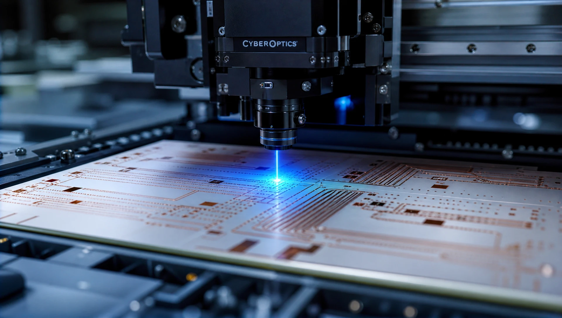
Manufacturing a multi-layer board entirely out of pure PTFE or Rogers laminates can be cost-prohibitive for commercial applications. To optimize the bill-of-materials (BOM) while maintaining high-frequency performance, leading high frequency pcb manufacturers design hybrid multi-layer stackups.
Combining dissimilar materials—such as Rogers RO4350B with standard High-Tg FR-4—introduces significant manufacturing complexity due to differing physical and thermal properties:
Coefficient of Thermal Expansion (CTE) Mismatch: PTFE materials exhibit a high Z-axis CTE (up to 130 ppm/deg C), whereas FR-4 features a Z-axis CTE of approximately 50 to 70 ppm/deg C. During reflow soldering (peak 260 deg C), uneven expansion can cause microvia shear, barrel cracking in plated through-holes, and internal layer delamination.
Lamination Temperature Profiles: FR-4 prepregs cure at approximately 175 deg C to 185 deg C, while certain pure PTFE bondply materials require lamination temperatures exceeding 220 deg C to 300 deg C. Hybrid lamination profiles must carefully balance dwell times, pressure ramping, and cooling rates to prevent resin starvation and severe board warp/twist.
Drilling and Desmear Chemistry: FR-4 and PTFE drill at different feed rates and speeds. Standard permanganate chemical desmear effective for FR-4 resin drill smear will not etch PTFE hole walls. A dual-stage desmear process utilizing plasma etching (tetrafluoromethane/oxygen gas plasma) is mandatory to clean and micro-roughen PTFE hole walls prior to copper plating.
At gigahertz frequencies, the choice of surface finish directly influences conductor loss, insertion loss, and long-term joint reliability.
Although ENIG provides excellent surface flatness for fine-pitch SMT pads, the electroless nickel layer (3 to 5 microns) is ferromagnetic and possesses higher electrical resistivity than copper. At frequencies above 5 GHz, skin depth dictates that the signal travels predominantly through this resistive nickel layer, significantly increasing insertion loss (often called the "nickel effect").
Immersion Silver deposits a thin (0.15 to 0.40 micron) layer of pure silver directly over copper. Silver exhibits higher electrical conductivity and lower resistivity than copper. Because no nickel intermediate layer is present, Immersion Silver delivers minimal insertion loss and exceptional phase stability across 10 GHz to 80 GHz mmWave frequencies.
ENEPIG replaces standard ENIG for complex hybrid builds requiring wire bonding (aluminum or gold wire) alongside SMT component reflow. The thin palladium layer reduces intermetallic corrosion ("black pad") while maintaining good high-frequency signal transmission.
| Surface Finish Option | Relative RF Loss (at > 10 GHz) | Co-planarity for SMT | Shelf Life | Wire Bonding Capability |
| Immersion Silver (IAg) | Lowest (Ideal) | Excellent | 6 - 12 Months | Aluminum Wire |
| Immersion Tin (ISn) | Low | Excellent | 6 Months | Limited |
| ENEPIG | Moderate | Excellent | 12+ Months | Gold & Aluminum |
| ENIG | High (Nickel Loss) | Excellent | 12+ Months | Aluminum Wire |
| HASL / Lead-Free HASL | Unacceptable (Uneven) | Poor | 12+ Months | Not Applicable |
Submitting Gerber, ODB++, or IPC-2581 datasets to a high frequency pcb manufacturer requires adhering to specific Design for Manufacturability (DFM) guidelines tailored to RF routing.
Mitering Sharp Bends: 90-degree trace bends cause local impedance discontinuities due to the increased trace width at the corner apex. Designers must use curved corners (radius >= 3 * trace width) or 45-degree mitered bends with an optimal miter fraction between 60% and 70%.
Via Fencing and Ground Stitching: To prevent lateral radiation and isolate RF traces from adjacent digital lines, stitch ground vias alongside microstrip or coplanar waveguide traces. The pitch between stitching vias must not exceed 1/10th of the highest operating signal wavelength in the substrate dielectric:
pitch_max <= c / (10 * f_max * sqrt(Dk))
Via Antipad Clearance Optimization: In multi-layer stripline configurations, signal vias passing through ground planes create parasitic capacitance. Enlarging the ground plane clearance (antipad) around the via barrel optimizes the via's TDR impedance profile, matching it to 50 ohms.
Backdrilling (Controlled-Depth Drilling): Unused via stubs in multi-layer boards act as open-ended transmission line stubs, causing severe resonant signal reflections at high frequencies. Backdrilling removes the inactive portion of plated through-holes, leaving a stub length of less than 0.20 mm (8 mils).
Validating high-frequency circuit boards requires advanced microwave test equipment beyond standard electrical continuity flying probe checks.
Time Domain Reflectometry (TDR) Coupon Testing: Test coupons added to the manufacturing panel are measured using high-bandwidth TDR oscilloscopes. A fast-rise-time step pulse is launched down the test trace to display characteristic impedance vs. distance, confirming that trace impedance falls within specified tolerance limits (e.g., 50 ohms +/- 5%).
Vector Network Analyzer (VNA) S-Parameter Verification: For ultra-high-frequency or mmWave projects, VNAs measure Scattering Parameters (S-parameters):
S11 (Return Loss): Measures reflected power at the input port.
S21 (Insertion Loss): Measures transmitted power through the transmission line.
Microsection Cross-Sectioning: Destructive analysis of test coupons verifies copper plating thickness inside via barrels (IPC Class 3 requires minimum average 25 microns / 1.0 mil), dielectric layer spacing, laminate adhesion, and copper etch profiles.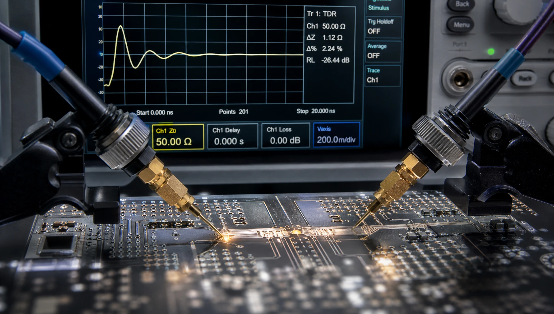
When evaluating partners on any high frequency pcb manufacturers list, procurement directors must evaluate technical capability matrices alongside quality accreditations and supply chain stability.
Does the fabricator maintain direct factory relationships with raw material suppliers? Procurement managers should confirm that the manufacturer sources genuine laminates from accredited foundries (e.g., Rogers Corporation, Taconic, Panasonic) rather than unverified generic equivalents.
Does the factory possess in-house plasma desmear capabilities? Processing pure PTFE or fluoropolymer substrates requires tetrafluoromethane/oxygen gas plasma chambers to etch hole walls before copper plating.
What is the factory's standard impedance control tolerance? A high-capability supplier should routinely achieve +/- 5% impedance tolerances on high-frequency builds using automated 2D field solver modeling and Laser Direct Imaging (LDI).
To justify investment in specialized high-frequency substrates and precision manufacturing workflows, procurement teams should evaluate performance, cost, and processing trade-offs.
| Manufacturing Parameter | Standard Commercial FR-4 PCB | High Frequency PCB (Rogers/PTFE) | Engineering & Strategic Impact |
| Operating Frequency Range | DC to 1 GHz | 1 GHz to 80+ GHz (mmWave) | Supports 5G, radar, satellite, and 100G networking. |
| Dielectric Constant (Dk) Stability | Poor (+/- 10% over frequency) | Exceptional (+/- 1% to 2%) | Maintains stable phase velocity and predictable impedance. |
| Dissipation Factor (Df) | High (~ 0.0200) | Ultra-Low (~ 0.0009 - 0.0037) | Prevents signal attenuation and board overheating. |
| Etching Tolerance Control | +/- 1.0 mil (+/- 0.025 mm) | +/- 0.5 mil (+/- 0.0125 mm) | Guarantees tight characteristic impedance (+/- 5%). |
| Hole Wall Desmear Method | Permanganate Chemical Wash | Plasma Etch (CF4 / O2) | Ensures copper plating adhesion on PTFE hole walls. |
| Surface Finish Selection | HASL, ENIG | Immersion Silver, ENEPIG | Eliminates skin-effect signal loss at high frequencies. |
High-frequency printed circuit board fabrication leaves no room for manufacturing error. Success requires precise substrate selection, field solver impedance modeling, advanced plasma processing, and rigorous TDR/VNA quality verification.
As an experienced high frequency pcb manufacturer, ApolloPCB offers end-to-end solutions for 5G telecommunications, aerospace, defense, automotive radar, and medical RF electronics. Our production facilities maintain high-speed LDI exposure units, multi-stage plasma desmear chambers, controlled-depth backdrilling machines, and high-bandwidth TDR impedance testing systems.
From quick-turn RF prototypes to high-volume IPC Class 3 multi-layer hybrid production, ApolloPCB guarantees precision engineering execution across every batch.
Streamline your RF manufacturing supply chain, prevent signal integrity failures, and accelerate your time-to-market. Contact our engineering team today to submit your Gerber files and stackup requirements.
Immersion Silver deposits pure silver directly onto copper without an intermediate magnetic nickel layer. Because signal current flows along the outer skin of traces at high frequencies, eliminating ENIG's resistive nickel layer prevents skin-effect signal attenuation, lowering insertion loss above 5 GHz.
ApolloPCB combines 2D boundary element field solvers during pre-production CAM engineering with Laser Direct Imaging (LDI) and precision vacuum etching line controls. Every panel is validated using Time Domain Reflectometry (TDR) coupon testing to confirm compliance before shipping.
A hybrid stackup places low-loss Rogers substrate layers exclusively on critical high-frequency signal routes, while utilizing cost-effective High-Tg FR-4 for internal power and low-speed control layers. This architecture preserves RF performance while reducing overall substrate material costs.

Got project ready to assembly? Contact us: info@apollopcb.com



 Whatsapp 0086 755 29438407
 Mail info@apollopcb.com
 Tel 0086 755 29438407


ABOUT US

PRODUCTS
TECHNOLOGY
KNOWLEDGE CENTRE
CULTURE
NEWS
We're not around but we still want to hear from you! Leave us a note:

Leave Message to APOLLOPCB
