




-
- PCB TYPE
- PRINTED CIRCUIT BOARD PROTOTYPE ALUMINUM PRINTED CIRCUIT BOARD R&F PCB FPC HIGH FREQUENCY PCB HIGH-TG PCB HEAVY COPPER PCB HDI PCB PCB FOR LIGHTING METAL CORE PCB


time:Aug 13. 2026, 13:46:20
In modern industrial manufacturing, printed circuit board assembly has evolved from simple component soldering into an integrated discipline combining materials science, automated micro-placement, thermal physics, and mechanical engineering. For factory OEMs, hardware engineering teams, and industrial procurement leaders, achieving zero-defect production requires managing a complex matrix of surface mount technology (SMT), mechanical integration, supply chain risk, and thermal profiling.
As microprocessors shrink and high-density interconnect (HDI) architectures become standard across industrial automation, automotive electronics, medical equipment, and telecommunications, selecting a qualified partner for pcb assembly is the single most critical factor determining product reliability and market success.
This guide provides hardware directors, manufacturing engineers, and B2B procurement managers with an actionable roadmap for managing contract manufacturing, optimizing assembly workflows, controlling bill-of-materials (BOM) costs, and ensuring full regulatory compliance across international markets.
To execute high-yield production runs, contract manufacturers utilize fully automated production lines governed by rigorous Design for Manufacturability (DFM) rules and automated optical inspections. Understanding each stage of the pcb assembly process allows engineering teams to optimize board layouts before committing to mass production.
Before a single component is loaded onto an SMT line, CAM engineers perform automated DFM audits. This step checks for footprint mismatches, solder mask clearances, thermal relief pad configurations, and component clearance distances to prevent solder bridging and tombstoning.
Laser-Cut Stencil Fabrication: Electro-polished stainless steel stencils are cut with step-down micro-apertures (for example, reducing thickness from 0.127 mm to 0.100 mm for 0201 passives or 0.4 mm pitch QFPs) to ensure precise solder paste release volumes.
Fiducial Mark Alignment: Board layouts must feature at least three global optical fiducials (1.0 mm to 1.5 mm bare copper pads with dark solder mask clearance) on panel corners to allow SMT vision systems to correct for rotational and translational offsets.
Over 60% of SMT assembly defects originate at the solder paste printing stage. Automated printers apply Type 4 or Type 5 lead-free solder pastes (such as SAC305) using squeegees operating at controlled angles, speeds, and down-pressures.
Directly after printing, 3D SPI systems scan 100% of the board pads using structured light projection. The SPI system measures:
Paste Volume Percentage: Ideal target range is 80% to 120% of calculated aperture volume.
Height Profile: Detects solder paste peaks, slumping, or uneven deposit thickness.
Offset Deviation: Flags XY position errors greater than 15% of pad dimensions.
Modern pick-and-place machines operate in multi-head gantry configurations capable of placing up to 100,000 components per hour (CPH). High-resolution vision systems verify component body dimensions, pin pitch, and ball grid array (BGA) coplanarity in real time prior to placement.
Component placement order follows a strict functional hierarchy:
Micro-passives (0201, 0402 footprints) and small discrete diodes.
Integrated Circuits (SOIC, QFP, QFN packages).
Ultra-fine pitch BGAs, Chip-Scale Packages (CSPs), and heavy mechanical connectors.
Board assemblies pass through multi-zone forced convection reflow ovens (typically 8 to 12 heating zones plus 2 cooling zones) blanketed with Nitrogen gas to minimize copper oxidation.
| Reflow Profile Stage | Target Temperature Range | Duration / Rate | Engineering Objective |
| Ramp-up Zone | Ambient to 150 deg C | 1.0 to 3.0 deg C / second | Prevents thermal shock to delicate ceramic passives |
| Soak Zone | 150 deg C to 200 deg C | 60 to 120 seconds | Equalizes board delta-T and fully activates flux |
| Reflow Zone | Peak 235 deg C to 245 deg C | 40 to 90 seconds above 217 deg C | Achieves complete alloy liquidus and pad wetting |
| Cooling Zone | Peak down to 100 deg C | -2.0 to -4.0 deg C / second | Forms fine intermetallic grain structure for joint strength |
For a detailed step-by-step breakdown of specialized automated SMT lines, read our
While SMT accounts for the vast majority of modern component placements, heavy-duty industrial control systems, power supplies, and automotive modules frequently require mixed-technology builds combining SMT with tht pcb assembly.
| Assembly Attribute | Surface Mount Technology (SMT) | Through-Hole Technology (THT) |
| Placement Method | High-speed automated pick-and-place | Automated insertion or manual lead positioning |
| Mechanical Joint Strength | Moderate (prone to shear stress) | Exceptional (anchored physically inside barrel) |
| Component Density | Extremely high (both top and bottom sides) | Low to moderate (requires large board footprint) |
| Power & Current Capacity | Low to moderate current density | High voltage and high current handling |
| Primary Component Types | MCUs, BGAs, QFNs, 0402/0201 passives | Transformers, relays, heavy terminal blocks, large electrolytic caps |
When assembling double-sided SMT boards that contain through-hole power connectors on one side, conventional wave soldering can damage delicate secondary-side surface-mount devices.
To overcome this, advanced factories employ selective soldering systems. A programmable nitrogen-shielded miniature solder fountain precisely targets individual through-hole pins from underneath the board, applying localized heat and solder without disturbing surrounding surface-mount devices.
To evaluate custom automated mixed-technology lines for industrial applications, explore our
Modern industrial design trendlines demand compact, lightweight, and vibration-resistant electronic enclosures. This shift has accelerated the adoption of flexible printed circuits and hybrid substrate architectures.
| Rigid-Flex Layer | Material Specification | Thickness Range | Functional Role in Stackup |
| Top Outer Cap | High-Tg FR-4 Glass Epoxy | 0.2 mm to 0.8 mm | Houses SMT components and outer mounting pads |
| Internal Layer 2 | Flexible Polyimide Core + Copper | 0.025 mm to 0.05 mm | Carries high-density signal traces across flexible zone |
| Internal Layer 3 | Flexible Polyimide Core + Copper | 0.025 mm to 0.05 mm | Serves as continuous ground/power plane reference |
| Bottom Outer Cap | High-Tg FR-4 Glass Epoxy | 0.2 mm to 0.8 mm | Provides structural rigidity for bottom SMT components |
Executing fpcb assembly (Flexible Printed Circuit Board Assembly) requires specialized tooling and mechanical stabilization protocols that differ significantly from standard rigid board processing:
Precision Carrier Pallets: Because flexible polyimide substrates (typically 0.025 mm to 0.05 mm core thickness) lack rigid structural support, they are mounted onto custom aluminum or composite vacuum fixture pallets using high-temperature polyimide tape or re-usable tacky gel surfaces to keep the substrate perfectly flat during paste printing and reflow.
Thermal Expansion Control: Polyimide exhibits a higher Coefficient of Thermal Expansion (CTE) and moisture absorption rate than standard glass-epoxy FR-4. Pre-baking flexible substrates at 100 deg C to 120 deg C for 2 to 4 hours prior to assembly drives out absorbed moisture, preventing layer delamination and blistering during 245 deg C lead-free reflow.
For dynamic environments such as medical endoscopes, aerospace gimbals, and industrial robotics, a 4 layer rigid-flex pcb assembly eliminates internal wire harnesses and board-to-board connectors, dramatically increasing mean time between failures (MTBF).
The minimum bend radius for rigid-flex installations is calculated as:
Minimum Bend Radius = Total Flex Core Thickness * Application Multiplier
Where the application multipliers are defined as:
Dynamic Flexing Applications (single-layer flex zone): Multiplier is greater than or equal to 60.
Static Flex-to-Install Applications (single-layer flex zone): Multiplier is greater than or equal to 10.
Static Flex-to-Install Applications (two-layer flex zone): Multiplier is greater than or equal to 15.
Discover detailed layer stackup options, adhesive-free flex materials, and mechanical layout constraints on our page dedicated to
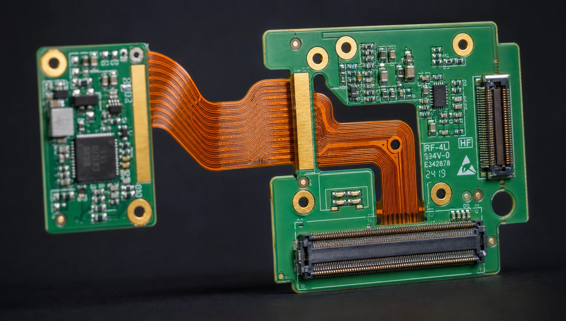
High-power industrial products, automotive ECU units, and outdoor LED lighting gear require direct structural fastening to metal chassis or heavy aluminum heatsinks. Achieving stable thermal dissipation and rigid structural mounting introduces specific mechanical machining requirements into the board assembly workflow.
A tapped counterbore in pcb assembly combines two distinct mechanical machining processes executed during the PCB fabrication and sub-assembly stage:
Counterbore Drilling: A two-stage drilling process creates a cylindrical, flat-bottomed recess that allows socket head cap screws or hex bolts to sit completely flush with or below the top surface of the circuit board.
Internal Thread Tapping: Precision mechanical taps cut internal threads into the wall of a plated through-hole or embedded brass collar. This allows mounting bolts to thread directly into the PCB assembly without requiring external locknuts on the reverse side.
Keep-Out Zones (KOZ): Mechanical tapping generates micro-swarf and high physical stresses. Designers must maintain a minimum 1.5 mm copper clearance radius around the outer rim of the counterbore to prevent internal layer short circuits or mechanical cracking of nearby ceramic capacitors (MLCCs).
De-burring and Cleaning: Automated high-pressure aqueous washing must clean tapped counterbores post-machining to remove microscopic metal filings before SMT components are placed, preventing random short circuits.
For hardware startups scaling to mass production as well as established factory procurement teams, managing the overall pcb assembly cost requires analyzing three primary cost drivers: Component NPI/Sourcing, Assembly Tooling, and Manufacturing Yield Rates.
| Cost Driver Category | Proportion of Total Assembly Cost | Key Variables & Impact Factors |
| Component BOM Sourcing | 55% - 70% | Turnkey vs consigned parts, minimum order quantities (MOQ), component lead times |
| Bare Board Substrate | 15% - 20% | Layer count, material choice (FR-4 vs Rogers/Flex), microvia density |
| SMT Setup & Tooling | 8% - 12% | Precision laser stencils, pick-and-place feeder setup fees, NPI programming |
| Testing & Quality Assurance | 5% - 10% | 3D AOI coverage, X-ray inspection for BGAs, custom ICT/FCT test fixture development |
Total contract manufacturing expenditure for an assembly production run can be calculated using the following engineering cost formula:
Total Assembly Cost = N_Units * (Cost_BOM + Cost_PCB) + Cost_NPI_Setup + Cost_Stencil + N_Units * (T_SMT * Rate_SMT + T_THT * Rate_THT + T_FCT * Rate_Testing)
Where:
N_Units = Total batch volume
Cost_BOM = Total Bill-of-Materials component cost per unit
Cost_PCB = Bare board fabrication unit cost
Cost_NPI_Setup = Non-recurring line engineering setup fee
Cost_Stencil = Precision laser-cut SMT stencil fee
T_SMT, T_THT, T_FCT = Cycle times per unit for SMT placement, THT soldering, and Functional Testing
Rate_SMT, Rate_THT, Rate_Testing = Hourly billing rates for automated lines, manual soldering operators, and testing stations
Standardize Passive Package Sizes: Replace disparate 0402, 0603, and 0805 resistors and capacitors with a single 0402 footprint across your design where voltage ratings permit. This reduces the number of pick-and-place feeder changeovers, reducing line setup times.
Panelization Efficiency: Design manufacturing panels (for example, 400 mm x 350 mm) with 10 mm waste tabs, breakaway v-scoring, or tab-routing with mouse bites to maximize panel utilization above 85%.
Consolidate SMT Components to One Side: Placing all surface-mount ICs and passives on the top side of the board eliminates a second SMT stencil, second paste printing pass, and second reflow oven cycle, reducing assembly labor fees by up to 35%.
For a deep-dive analysis of turn-key material sourcing versus consigned component models, review our
Exporting commercial electronic equipment to European, North American, and Asian markets mandates strict compliance with environmental protection directives and industrial quality benchmarks.
Executing a rohs compliant pcb assembly process requires complete segregation of leaded and lead-free production materials within the manufacturing facility:
Lead-Free Solder Alloys: Standard lead-free production utilizes SAC305 (96.5% Tin, 3.0% Silver, 0.5% Copper) or Sn100C (Tin-Copper-Nickel-Bismuth alloy) solder pastes with melting points around 217 deg C to 227 deg C.
Material Traceability & Certificates of Conformance (CoC): Every component line item on the BOM must be verified against manufacturer datasheets for RoHS compliance, ensuring that internal lead-frame plating, IC packaging mold compounds, and passive terminations are lead-free.
Bare Board Surface Finish Selection: PCB fabricators must apply lead-free surface finishes such as Electroless Nickel Immersion Gold (ENIG), Immersion Silver (IAg), or Lead-Free HASL (Hot Air Solder Leveling) to prevent lead contamination.
| Defect Category | Visual Manual Inspection | 3D Automated Optical Inspection (AOI) | Automated X-Ray Inspection (AXI) |
| Solder Bridging | Moderate Detection Rate | High Detection Rate | High Detection Rate |
| Component Tombstoning | High Detection Rate | High Detection Rate | High Detection Rate |
| BGA Voiding (> 15%) | Undetectable | Undetectable | High Detection Rate (Essential) |
| Inverted Polarity | Low Detection Rate | High Detection Rate | Moderate Detection Rate |
| De-wetting / Cold Joint | Low Detection Rate | High Detection Rate | High Detection Rate |
1.3D Automated Optical Inspection (AOI): Positioned post-reflow, 3D AOI uses multi-angle LED illumination and high-resolution cameras to capture topographic 3D mesh projections of solder joints, detecting lifted leads, missing components, incorrect polarity, and solder volume anomalies.
2.Automated X-Ray Inspection (AXI): For Quad Flat No-lead (QFN) packages and Ball Grid Arrays (BGAs) where solder joints are hidden beneath the component body, AXI inspects solder coverage and checks for internal voiding. IPC Class 2 standards mandate that total voiding within a BGA solder ball must not exceed 25% of the total ball area.
To learn more about selecting audited contract manufacturers with full compliance certifications, review our ranking of
When sourcing a reliable supplier for turnkey pcb assembly manufacturing, procurement teams should conduct a rigorous vendor audit assessing technical capabilities, quality management certifications, and engineering support services.
| Evaluation Criterion | Target Capability Standard | Impact on OEM Quality |
| Factory Certifications | ISO 9001:2015, ISO 13485 (Medical), IATF 16949 (Automotive) | Validates formal quality management systems |
| Component Supply Chain | Direct authorized distributor network (DigiKey, Mouser, Arrow) | Prevents grey-market counterfeit components |
| Placement Capabilities | Down to 01005 passives; fine-pitch BGA down to 0.3 mm pitch | Enables high-density component integration |
| In-Line Quality Testing | 3D SPI, 3D AOI, 3D AXI, ICT, and custom FCT stations | Guarantees first-pass yield above 99.5% |
| Turnaround Velocity | Quick-turn prototype (24-48 hours), Mass Production (2-3 weeks) | Shortens hardware development cycle times |
Partnering with an established manufacturer guarantees end-to-end component traceability, structured DFM engineering feedback, and high first-pass yield rates across complex multi-layer builds.
To evaluate our certified SMT facilities, cleanroom capabilities, and full OEM service offerings, visit our dedicated portal for
Executing high-reliability electronics manufacturing demands strict control across every phase of production:
Engineering Pre-Check: Perform 3D SPI and CAM DFM audits to eliminate paste defects and layout errors before production starts.
Advanced Substrate Integration: Leverage dynamic flex protocols for fpcb assembly and 4 layer rigid-flex pcb assembly to reduce mechanical connector failures.
Precision Machining: Incorporate tapped counterbore in pcb assembly features to improve mechanical housing integration and direct thermal anchoring.
Environmental & Cost Control: Enforce rohs compliant pcb assembly standards while optimizing component package choices to keep the overall pcb assembly cost competitive.
As a certified leader in pcb assembly and manufacturing, ApolloPCB provides complete turn-key solutions—from component procurement and bare-board fabrication to automated SMT, through-hole assembly, and functional testing.
Accelerate your hardware development cycle, eliminate manufacturing defects, and lower your total procurement costs.
ApolloPCB operates high-speed SMT lines equipped with high-resolution vision systems capable of placing ultra-fine pitch components down to 0.3 mm pitch for BGAs/CSPs and discrete passive components down to 01005 footprints.
ApolloPCB maintains direct procurement contracts with original component manufacturers and authorized global distributors (such as DigiKey, Mouser, and Arrow). Incoming shipments undergo visual verification, solderability testing, and optional X-ray die inspection.
Yes, ApolloPCB maintains dedicated, environmentally segregated SMT reflow and wave soldering lines specifically for RoHS compliant lead-free processing (SAC305) to eliminate cross-contamination risks for international export compliance.

Got project ready to assembly? Contact us: info@apollopcb.com



 Whatsapp 0086 755 29438407
 Mail info@apollopcb.com
 Tel 0086 755 29438407


ABOUT US

PRODUCTS
TECHNOLOGY
KNOWLEDGE CENTRE
CULTURE
NEWS
We're not around but we still want to hear from you! Leave us a note:

Leave Message to APOLLOPCB
