




-
- PCB TYPE
- PRINTED CIRCUIT BOARD PROTOTYPE ALUMINUM PRINTED CIRCUIT BOARD R&F PCB FPC HIGH FREQUENCY PCB HIGH-TG PCB HEAVY COPPER PCB HDI PCB PCB FOR LIGHTING METAL CORE PCB


time:Aug 10. 2026, 17:48:36
Global industrial original equipment manufacturers (OEMs), automotive hardware designers, and high-reliability system integrators routinely face a complex engineering challenge: how to combine ultra-fine-pitch microelectronics with heavy-duty electromechanical components on a single circuit board. While Surface Mount Technology (SMT) dominates modern electronic design due to its high density and automated placement efficiency, Through-Hole Technology (THT) remains indispensable for power delivery, high-stress connectors, relays, and large electrolytic capacitors.
Executing high-yield mixed-technology pcb production requires a deep understanding of thermal dynamics, dual-stage soldering workflows, design for manufacturability (DFM) rules, and automated inline inspection protocols. Combining SMT and THT components on the same substrate introduces thermal mismatches, shadow effects during wave soldering, and strict clearance constraints that can compromise product reliability if not properly managed.
This technical engineering guide provides factory buyers, procurement managers, and hardware directors with an actionable framework for mastering mixed-technology printed circuit board manufacturing. We examine processing sequences, thermal management strategies, DFM layout tolerances, IPC quality acceptance criteria, and cost-reduction strategies for high-reliability industrial builds.
Mixed-technology PCB production refers to the fabrication and assembly of printed circuit boards that integrate both Surface Mount Devices (SMDs) and Through-Hole Components (THCs) on the same board assembly. Rather than relying exclusively on SMT reflow or conventional THT wave soldering, mixed assembly requires a unified, multi-stage manufacturing line capable of processing vastly different component geometries, thermal masses, and terminal configurations.
Modern industrial equipment—such as variable frequency drives (VFDs), solar inverters, medical imaging systems, and automotive electronic control units (ECUs)—demands high computational density alongside robust mechanical strength.
Mechanical Retention and Strain Relief: Heavy connectors, terminal blocks, and switches subjected to repetitive physical plugging or mechanical vibration require the mechanical anchoring strength provided by plated through-hole (PTH) barrels.
Power Electronics and Heat Dissipation: High-current inductors, power MOSFETs mounted to heat sinks, and industrial relays generate significant heat and carry high amperage. Through-hole leads provide low electrical resistance and efficient heat transfers into internal copper planes.
Component Availability: Legacy integrated circuits, specialized transformers, and industrial sensors are often manufactured exclusively in through-hole pin formats, forcing hybrid layouts.
To review the specific production efficiencies, thermal performance characteristics, and cost structures of hybrid circuit layouts, explore our detailed technical analysis on
The complexity of mixed-technology manufacturing depends directly on the physical arrangement of components across the top and bottom layers of the board. Manufacturing engineers categorize hybrid boards into three distinct assembly classes:
Configuration: Surface-mount components and through-hole components are populated exclusively on the top side of the board substrate.
Processing Sequence: Solder paste printing -> SMT pick-and-place -> Reflow soldering -> THT component insertion -> Wave soldering or selective soldering.
Application: Standard consumer electronics, power supply control cards, and low-cost sensor modules.
Configuration: SMT components reside on both the top and bottom sides, while through-hole components are restricted to the top side.
Processing Sequence: Top-side solder paste printing -> Top SMT placement -> Top reflow -> Bottom-side solder paste printing (or glue dispensing) -> Bottom SMT placement -> Bottom reflow -> Top THT insertion -> Selective wave soldering.
Application: Automotive ECUs, industrial controllers, motor drives, and telecom infrastructure.
Configuration: Complex assemblies featuring SMT and THT components on both upper and lower substrate layers.
Processing Sequence: Multi-pass SMT reflow cycles combined with localized selective soldering, wave solder masking/pallets, or robotic point-to-point soldering.
Application: High-density aerospace hardware, defense electronics, and specialized medical diagnostic equipment.
| Manufacturing Attribute | Type I (Single-Side Mixed) | Type II (Double-Side SMT + THT) | Type III (Complex Double-Side) |
| Process Steps Count | 5 to 7 Process Steps | 8 to 11 Process Steps | 12+ Process Steps |
| Thermal Cycles | 1 Reflow + 1 Wave | 2 Reflows + 1 Wave | 2+ Reflows + Selective/Robot |
| Tooling Requirements | Standard SMT Stencil | SMT Stencils + Wave Pallets | Custom Selective Nozzles/Pallets |
| Defect Sensitivity | Low to Moderate | Moderate to High | High (Requires 100% Inspection) |
| IPC Quality Fit | Class 1 & Class 2 | Class 2 & Class 3 | Class 3 High-Reliability |
Achieving zero-defect yield during mixed-technology pcb production requires precise process execution. The manufacturing pipeline combines high-speed surface-mount placement with controlled thermal soldering for through-hole pin insertion.
                    DOUBLE-SIDED MIXED ASSEMBLY WORKFLOW
                                     │
   ┌─────────────────────────────────┘
   ▼
[ Step 1: Top-Side SMT Paste Printing & 3D SPI ]
   │
   ▼
[ Step 2: High-Speed Pick-and-Place (Chip Shooters & Flexible Placer) ]
   │
   ▼
[ Step 3: Convection Reflow Soldering (N2 Atmosphere, 10-12 Zones) ]
   │
   ▼
[ Step 4: Inverted Board Flip & Bottom-Side SMT Assembly ]
   │
   ▼
[ Step 5: Automated 3D AOI & Inline X-Ray Inspection (AXI) ]
   │
   ▼
[ Step 6: Manual / Robotic THT Component Insertion ]
   │
   ▼
[ Step 7: Selective Wave Soldering or Wave Pallet Soldering ]
   │
   ▼
[ Step 8: Ionic Contamination Wash & Final Electrical Test (ICT/FPT) ]
Solder Paste Printing and 3D SPI: Lead-free SAC305 or SnPb solder paste is applied via laser-cut electro-polished stainless steel stencils. A 3D Solder Paste Inspection (SPI) system measures paste volume, area, height, and alignment off-set before component placement.
High-Speed Pick-and-Place: High-speed chip shooters place 0201/0402 passives, while multi-axis flexible placers align fine-pitch BGAs, QFNs, and quad-flat packages (QFPs) using vision alignment systems.
Multi-Zone Convection Reflow: Boards pass through a 10-to-12-zone reflow oven under a nitrogen atmosphere. The temperature profile is carefully controlled to maintain soak times between 150 degrees C and 180 degrees C, reaching a peak temperature of 235 degrees C to 245 degrees C for SAC305 alloy.
Once SMT reflow is complete and verified via Automated Optical Inspection (AOI), through-hole components are integrated into the assembly:
Component Insertion: Radial and axial components are inserted using automated insertion machinery, while heavy connectors, switches, and large transformers are populated via ergonomic manual assembly stations or collaborative assembly robots.
Selective Soldering vs. Full Wave Soldering:
Full Wave Soldering: Used when bottom-side SMT components are absent or encapsulated in wave-solder protective pallets. The entire board underside contacts a molten solder wave.
Selective Soldering: A programmable miniature solder fountain targets individual THT leads from underneath without exposing adjacent bottom-side SMT passives or fine-pitch ICs to direct solder waves.
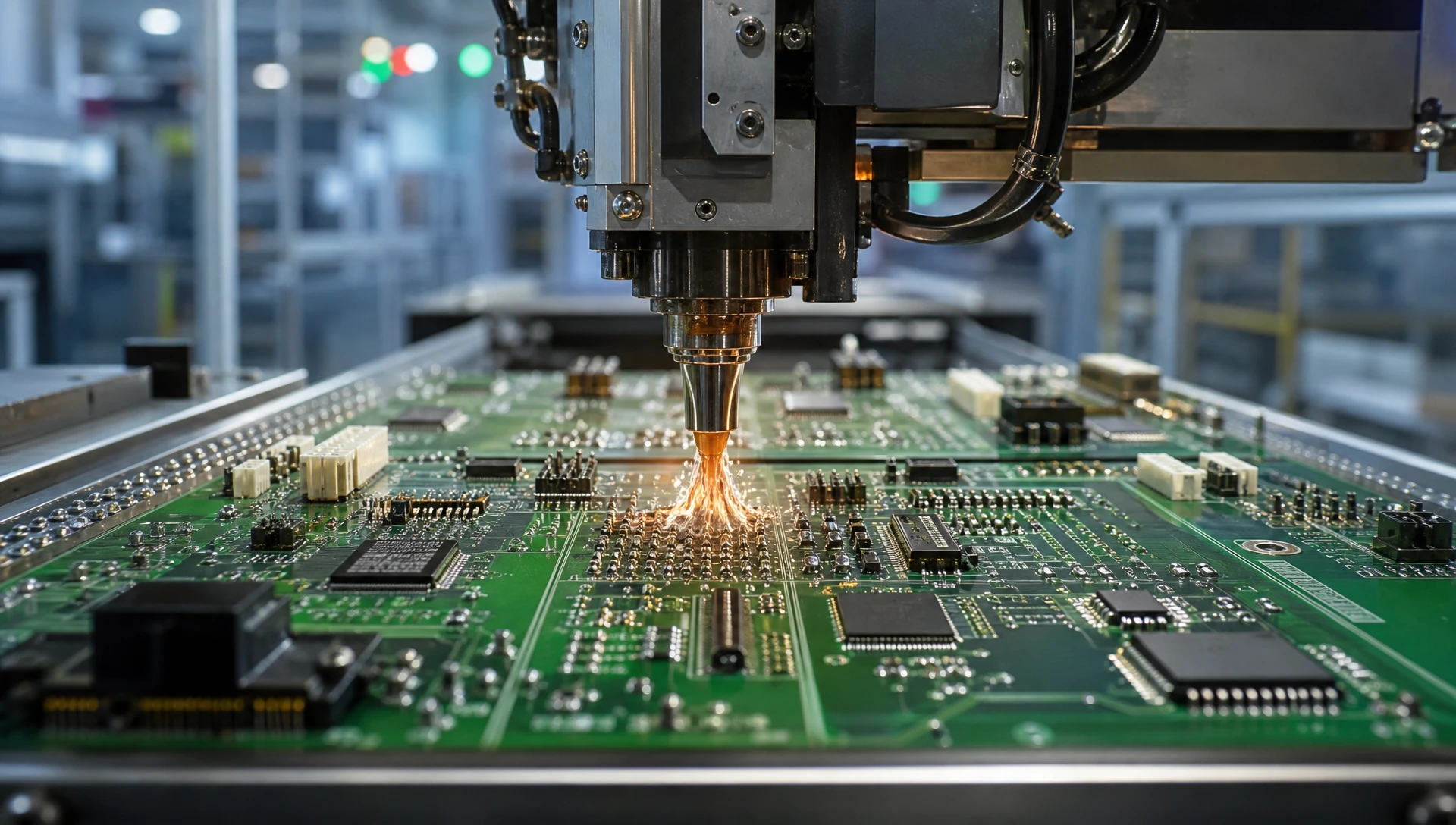
To reduce manual labor costs and eliminate wave-soldering passes, advanced manufacturers use Pin-in-Paste (PiP) technology—also known as Intrusive Reflow or Through-Hole Reflow (THR).
                      PIN-IN-PASTE (INTRUSIVE REFLOW) DYNAMICS

  1. Paste Overprint               2. THT Pin Insertion            3. Post-Reflow Fillet
  ┌───┐       ┌───┐               ┌───┐       ┌───┐               ┌───┐       ┌───┐
  │░░░│       │░░░│               │░░░│   │   │░░░│               │██│   │   │██│
 ─┴───┴───────┴───┴─             ─┴───┴───┼───┴───┴─
   │ PTH Barrel │                   │ PTH │ Pin │                   │ Solid Fillet │
 ─┬───┬───────┬───┬─             ─┬───┬───┼───┬───┬─
  │░░░│       │░░░│               │░░░│   │   │░░░│               │██│   │   │██│
  └───┘       └───┘               └───┘       └───┘               └───┘       └───┘
In a Pin-in-Paste workflow, high-volume solder paste is deposited directly into and over plated through-hole barrels using specialized stencil apertures (often step-down or overprinted stencils). Through-hole component leads are inserted through the wet paste. When the entire board passes through the standard SMT reflow oven, the solder paste melts, wicks into the barrel by capillary action, and forms a solid structural fillet around the THT lead.
To ensure full barrel fill (IPC Class 3 mandates 100% vertical fill; IPC Class 2 mandates 75%), manufacturing engineers calculate the required wet paste overprint volume using the volume equation:
V_paste = (V_hole - V_lead) / S_shrink
Where:
V_paste = Total required volume of printed wet solder paste.
V_hole = Volume of the internal plated through-hole barrel.
V_lead = Volume of the inserted component pin within the barrel region.
S_shrink = Solder paste solid metal fraction (typically 0.50 or 50% for standard pastes containing 50% flux vehicle by volume).
Component Temperature Resistance: Through-hole plastic headers and bodies must withstand full convection reflow profiles (up to 260 degrees C peak for 30 to 40 seconds) without warping, melting, or degrading.
Lead Length Control: Pin protrusion below the board edge must not exceed 1.5 mm. Excessively long pins push wet solder paste out of the bottom of the barrel during insertion, causing solder starvation and insufficient vertical fill.
Mixed-technology board manufacturing presents unique thermal management challenges due to the massive heat capacity differential between discrete 0402 chip resistors and large metal-shielded industrial power relays or transformers.
During convection reflow, low-mass SMT components heat quickly, while high-mass THT components lag behind. This creates a temperature differential across the substrate.
Preventing Cold Solder Joints: If a high-mass THT pin fails to reach liquidus temperature (217 degrees C for SAC305) during the reflow window, the solder will not wet the pin properly, causing a high-resistance cold solder joint.
Mitigating Thermal Stress and Board Warpage: Uneven heating across multi-layer stackups with heavy internal copper planes (e.g., 2 oz or 3 oz copper layers) induces localized stress. This leads to substrate bowing, twist, and micro-cracking inside plated through-hole walls.
Extended Reflow Soak Profiles: Implement a prolonged soak zone (150 degrees C to 180 degrees C for 90 to 120 seconds) in the reflow oven. This equilibrates temperatures across high-mass and low-mass components before raising the board to peak liquidus.
Selective Thermal Relief Pad Design: Connect internal power and ground copper planes to through-hole pads using thermal relief geometries (4-spoke or 2-spoke patterns) rather than solid copper pours. This prevents heat from sinking away from the joint during soldering.
Implementing comprehensive DFM checks during the initial layout phase eliminates layout redesigns, prevents component shadow defects during wave soldering, and maximizes production yield.
SMD-to-PTH Annular Clearance: Maintain a minimum distance of 2.0 mm (80 mils) between bottom-side SMT component pads and through-hole component pads. This provides adequate clearance for selective solder nozzles and prevents bridging during wave soldering.
Wave Solder Component Orientation: Align rectangular bottom-side SMT passive components (0805, 1206) with their long axes perpendicular to the direction of wave travel. This ensures both terminations contact the molten solder wave simultaneously, preventing tombstoning and single-ended solder starvation.
Lead Protrusion Proximity: Ensure through-hole component pins extend between 0.5 mm and 1.5 mm beyond the bottom side of the substrate. Pins shorter than 0.5 mm fail to form complete bottom fillets, while pins longer than 2.0 mm interfere with selective solder nozzles and wave pallets.
Solder Mask Dam Clearances: Maintain a minimum green solder mask dam width of 0.10 mm (4 mils) between adjacent fine-pitch SMT pads and through-hole annular rings to prevent solder migration and short circuits.
| DFM Design Parameter | Minimum Standard | Recommended Industrial | Class 3 High-Reliability |
| SMD to PTH Pad Distance | 1.25 mm (50 mils) | 2.00 mm (80 mils) | 3.00 mm (120 mils) |
| PTH Annular Ring Protrusion | 0.125 mm (5 mils) | 0.25 mm (10 mils) | 0.35 mm (14 mils) |
| BGA Distance to Wave Region | 3.00 mm (120 mils) | 5.00 mm (200 mils) | 10.00 mm (400 mils) |
| PiP Hole-to-Pin Diameter Ratio | Pin + 0.15 mm | Pin + 0.25 mm | Pin + 0.20 mm |
| Edge Clearance (Conveyor Rail) | 3.00 mm | 5.00 mm | 7.50 mm |
Validating mixed-technology printed circuit board assemblies requires specialized inspection techniques. SMT solder joints are evaluated primarily from above, while through-hole leads require volumetric barrel inspection.
Factory procurement teams must specify the required IPC acceptance class prior to production:
IPC Class 2 (Dedicated Service Electronic Products): Covers commercial equipment, industrial controllers, and communication hardware. Requires a minimum of 75% vertical solder barrel fill in plated through-holes, with acceptable surface wetting across 270 degrees of the pin circumference.
IPC Class 3 (High-Performance / Harsh Environment Electronics): Mandatory for aerospace, life-support medical devices, defense systems, and severe industrial environments. Demands 100% vertical barrel fill, 360-degree circumferential wetting on top and bottom destination sides, and strict voiding limits (< 15% total void area in BGA solder balls).
Top and Bottom 3D AOI: Multi-camera 3D optical inspection platforms measure solder fillet height, component coplanarity, part presence, orientation, and leg lifting across all surface-mount devices.
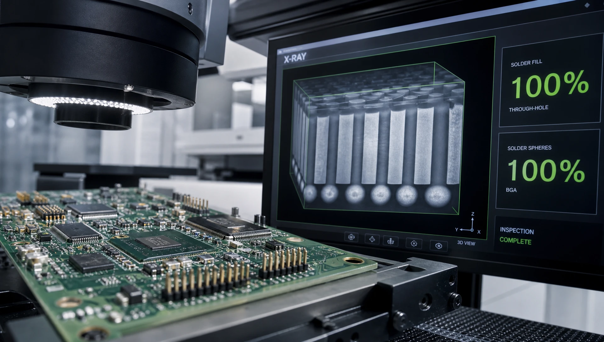
Automated X-Ray Inspection (AXI): Transmissive and tomographic 3D X-ray systems penetrate dense substrates to inspect hidden solder connections under BGA packages, Quad-Flat No-Lead (QFN) thermal ground pads, and internal through-hole barrel fill percentages for Pin-in-Paste components.
In-Circuit Testing (ICT) and Flying Probe: Dedicated bed-of-nails or high-speed flying probe needle fixtures verify component values, check for open circuit traces, detect shorts, and validate active IC bias voltages.
Resistivity of Solvent Extract (ROSE) Testing: Measures ionic contamination levels across the board surface to ensure no conductive flux residue remains before applying conformal coatings.
 8. Sourcing, Supply Chain Optimization, and Cost Reduction
Managing mixed-technology pcb production requires procurement teams to optimize bill-of-materials (BOM) structures, reduce manual assembly steps, and establish robust material traceability.
Convert THT to Pin-in-Paste Where Feasible: Work with design teams to replace hand-soldered THT connectors with reflow-compatible intrusive reflow parts. Eliminating a secondary wave soldering operation reduces unit assembly labor costs by 15% to 25%.
Standardize Component Packaging Formats: Procure SMT passives in continuous 7-inch or 13-inch tape-and-reel formats rather than cut tape. Supply THT components in ammo-packs or tape-and-reel for automated insertion equipment to maximize line uptime.
Optimize Selective Wave Tooling: For high-volume production runs, invest in multi-cavity titanium wave soldering pallets or custom selective solder nozzle plates to process multiple circuit boards simultaneously.
Implement Full Traceability Systems: Require your manufacturing partner to maintain lot-level traceability linking individual component reel batch numbers, solder paste batch IDs, reflow temperature profiles, and 3D AOI inspection records to unique 2D DataMatrix barcodes etched onto each PCB substrate.
When planning production budgets, evaluating assembly alternatives ensures the optimal balance between initial NRE tooling costs and long-term production efficiency.
| Assembly Metric | Manual THT Hand Soldering | Standard Wave Soldering | Selective Wave Soldering | Intrusive Reflow (Pin-in-Paste) |
| Initial NRE / Tooling Cost | Very Low ($0) | Moderate ($300 - $800 Pallet) | Moderate ($500 - $1,500 Nozzle) | Low ($100 Stencil Adjustment) |
| Throughput Speed | Low (Slow Manual Pace) | High (Continuous Conveyor) | Moderate to High | Very High (Equal to SMT Line) |
| Solder Joint Consistency | Variable (Operator Dependent) | Good (Process Controlled) | Excellent (Programmable) | Superior (Automated Paste Volume) |
| Thermal Stress on Board | Localized High Stress | High (Entire Board Exposed) | Low (Localized Target Heat) | Standard SMT Profile Exposure |
| Defect Rate (DPMO) | High (100 - 300 DPMO) | Moderate (20 - 50 DPMO) | Very Low (< 10 DPMO) | Extremely Low (< 5 DPMO) |
| Best Volume Application | Low-Volume Prototyping | High-Volume Uniform Builds | Complex Double-Sided SMT | High-Density Automated Runs |
Successfully manufacturing mixed-technology circuit boards requires tight coordination between design specifications, thermal process controls, and IPC quality standards. By optimizing DFM rules, selecting the right assembly methods, and enforcing strict 3D AOI/AXI inspection, industrial OEMs can achieve zero-defect quality while minimizing overall assembly costs.
As a certified turnkey manufacturing partner, ApolloPCB operates automated dual-sided SMT lines, programmable selective wave soldering stations, 3D SPI/AOI platforms, and high-resolution inline X-ray inspection equipment. From prototype builds to high-volume IPC Class 3 industrial production, ApolloPCB delivers end-to-end quality assurance across every build.
Ready to optimize your hybrid circuit board assembly? Submit your Gerber engineering files, component drawings, and bill of materials to receive a detailed DFM evaluation and quote.
Mixed-technology PCB production allows industrial OEMs to combine high-density microelectronics (BGAs, fine-pitch SMT) with high-strength, high-power through-hole components (connectors, relays, large capacitors) on a single substrate, maximizing functional capability without sacrificing mechanical reliability.
Pin-in-Paste (intrusive reflow) allows through-hole components to be soldered during the standard SMT reflow process. Solder paste is overprinted into plated through-hole barrels, component pins are inserted, and the entire assembly is reflowed together. This eliminates the need for wave soldering passes, significantly reducing manual assembly labor.
ApolloPCB utilizes 3D Automated Optical Inspection (AOI) alongside inline Automated X-Ray Inspection (AXI). AXI non-destructively penetrates dense components and substrates to inspect hidden BGA solder balls, detect internal voids, and measure vertical solder barrel fill percentages inside through-holes to guarantee compliance with IPC Class 2 and Class 3 standards.

Got project ready to assembly? Contact us: info@apollopcb.com



 Whatsapp 0086 755 29438407
 Mail info@apollopcb.com
 Tel 0086 755 29438407


ABOUT US

PRODUCTS
TECHNOLOGY
KNOWLEDGE CENTRE
CULTURE
NEWS
We're not around but we still want to hear from you! Leave us a note:

Leave Message to APOLLOPCB
