




-
- PCB TYPE
- PRINTED CIRCUIT BOARD PROTOTYPE ALUMINUM PRINTED CIRCUIT BOARD R&F PCB FPC HIGH FREQUENCY PCB HIGH-TG PCB HEAVY COPPER PCB HDI PCB PCB FOR LIGHTING METAL CORE PCB


time:Aug 17. 2026, 09:55:17
Selecting the appropriate substrate material is the foundation of high-performance LED circuit board design. Excessive junction temperatures reduce LED luminous efficacy, cause color temperature shifts (chromaticity drift), and accelerate lumen depreciation. Contract manufacturers must provide diverse material capabilities tailored to specific thermal and mechanical operating conditions.
| Substrate Type | Thermal Conductivity (W/m·K) | Dielectric Layer Options | Primary Lighting Applications | Key Manufacturing Advantages |
| Aluminum Metal Core (MCPCB) | 1.0 - 8.0 | Thermally conductive polymer | High-bay industrial lights, LED streetlights, automotive lighting | Superior heat dissipation, cost-effective structural strength |
| Copper Core (DTP / Non-DTP) | 2.0 - 400.0 | Direct Thermal Path (DTP) bare copper pad | Ultra-high-power stadium lighting, searchlights, COB modules | Lowest thermal resistance, maximum LED junction lifespan |
| High-Tg FR-4 Glass-Epoxy | 0.3 - 0.8 | Standard epoxy glass matrix (Tg >= 170°C) | Low-power commercial downlights, smart ambient light bars | Multilayer routing capability, low material cost |
| Flexible Polyimide Substrate | 0.2 - 0.5 | Thin adhesive or adhesive-free polyimide | Flexible LED strips, curved automotive taillights, dynamic displays | Ultra-lightweight, 3D contour fitting, high fatigue resistance |
| Ceramic Substrate (Al2O3 / AlN) | 24.0 - 180.0 | Direct Bonded Copper (DBC) / Thick Film | High-density chip-on-board (COB), UV-C LED sterilization | Zero CTE mismatch with LED chips, extreme dielectric isolation |
Metal Core PCBs represent the industry standard for high-flux commercial and industrial LED lighting. An aluminum MCPCB consists of three distinct functional layers:
Base Aluminum Layer: Typically 5052 or 6061 alloy aluminum plates ranging from 0.8 mm to 3.0 mm in thickness, providing mechanical rigidity and efficient thermal spreading.
Thermally Conductive Dielectric Layer: A specialized polymer composite filled with ceramic micro-particles (e.g., alumina or boron nitride). This layer provides high electrical insulation (> 3000V AC) while maintaining low thermal impedance.
Copper Circuit Layer: Heavy copper foil (1 oz to 5 oz) etched into circuit traces capable of carrying sustained current to high-voltage LED strings.
For extreme power density applications exceeding 10W per LED component, standard dielectric layers create a thermal bottleneck. Direct Thermal Path (DTP) copper substrates eliminate the dielectric insulator directly under the thermal pad of the LED package.
By soldering the LED’s thermal slug directly to a solid copper pillar (400 W/m·K conductivity), junction heat bypasses the insulation layer entirely and flows straight into the primary heat sink.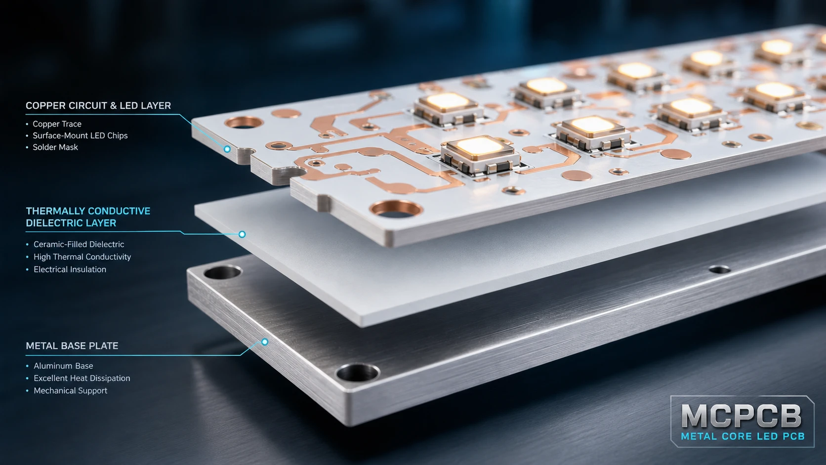
An advanced manufacturing facility must maintain tight tolerances across material processing, layer lamination, and mechanical finishing. The following parameters define world-class production capabilities for industrial-grade LED circuit boards.
Thermal Conductivity Range: Standard production spans 1.0 W/m·K to 8.0 W/m·K. High-end formulations utilize nano-ceramic filled polymers to achieve minimal thermal resistance (< 0.10°C·in²/W).
Dielectric Breakdown Voltage: High-power LED arrays operating on high-voltage DC buses require isolation ratings from 3000V AC up to 6000V AC to pass UL 8750 and EN 60598 safety certifications.
Insulation Layer Thickness: Standard layer thickness ranges from 50 µm to 150 µm. Thinner dielectric layers reduce thermal resistance but require precise lamination control to prevent pinhole breakdown under high voltage.
Industrial LED lighting drivers and high-density arrays generate high amperage spikes. Production capabilities must accommodate heavy copper weights:
Current Capacity Factor = Cross-Sectional Trace Area * Temperature Rise Limit * Copper Purity Factor
Standard Copper Weight: 1 oz (35 µm) and 2 oz (70 µm) for commercial ambient lighting.
Heavy Copper Capabilities: Up to 10 oz (350 µm) for high-amperage industrial LED driver boards, embedded power converters, and automotive matrix controllers.
Etching Tolerances: Fine-line trace/space capability down to 3.5 mil / 3.5 mil (90 µm) on 1 oz copper, ensuring compact board layouts for micro-LED arrays.
V-Scoring Precision: Computer-controlled V-score machines maintain depth tolerances of ±0.05 mm on aluminum and copper substrates, preventing edge burrs during manual or automated depanelization.
CNC Routing & Counterboring: High-speed CNC routers equipped with diamond-coated carbide bits cut complex outline geometries, sink routing, and mounting holes for chassis attachment.
Punching & Stamping: High-speed mechanical punching dies process high-volume aluminum LED panels up to 2.0 mm thickness with tight edge tolerances.
The assembly process for LED printed circuit boards requires specialized equipment configurations to prevent physical damage to silicone lenses, maintain accurate color binning, and avoid thermal stress during reflow.
Electro-Polished Stencils: Step-down laser-cut stencils (e.g., 100 µm to 120 µm) ensure accurate solder paste volumes on fine-pitch LED pads, preventing solder bead generation under high-power LED packages.
3D Solder Paste Inspection (SPI): 100% inline volumetric inspection ensures zero dry-joint or bridging defects prior to component placement, maintaining a height accuracy within ±5 µm.
Modern LED assembly equipment must manage delicate optical components without applying excessive vertical force or off-center torque:
Vacuum Nozzle Design: Soft rubber or Teflon-coated vacuum nozzles grip the outer perimeter of the LED casing, avoiding direct contact with soft silicone optical domes.
Optical Alignment Systems: High-resolution vision algorithms detect registration marks on the component body rather than the flexible lens, ensuring placement accuracy within ±0.025 mm.
LED Binning Management: Barcode-integrated feeder systems track MacAdam ellipse color temperature bins (1-step, 3-step, or 5-step binning), ensuring uniform color appearance across large lighting panels.
Reflow profiles for LED assemblies must balance full alloy liquidus wetting with strict thermal limits to avoid yellowing the silicone lens or degrading the internal wire bonds.
| Profile Zone | Temperature Range | Dwell Time / Ramp Rate | Thermal Objective |
| Preheat Zone | 120°C - 160°C | 1.0 - 2.5°C/sec | Evaporates paste solvents, prevents thermal shock |
| Soak Zone | 160°C - 200°C | 60 - 120 seconds | Equalizes temperature delta across aluminum board mass |
| Reflow Zone | Peak 235°C - 245°C | 30 - 60 seconds (> 217°C) | Achieves complete SAC305 alloy liquidus without lens discoloration |
| Cooling Zone | Peak down to 100°C | 2.5 - 4.0°C/sec | Forms fine intermetallic grain structure for joint fatigue resistance |

As architectural and automotive lighting designs push toward curved surfaces, narrow profiles, and moving mechanical joints, conventional rigid aluminum boards are supplemented by dynamic hybrid designs.
Integrating dynamic flexible circuitry directly into rigid control boards eliminates board-to-board wiring harnesses, slashes assembly labor, and improves mechanical vibration resistance in demanding environments. For comprehensive design parameters on dynamic substrate bending, explore our
Layer Stackup Versatility: 2-layer to 12-layer hybrid rigid-flex configurations integrating FR-4 stiffeners, copper layers, and polyimide cores.
Dynamic Bend Radius: Designed for dynamic flexing installations with a minimum bend radius up to 10 times the flex core thickness, making it ideal for robotic arms and linear architectural contours.
Surface Finish Options: Electroless Nickel Immersion Gold (ENIG), Immersion Silver (IAg), and Direct Immersion Gold (DIG) to ensure maximum solderability and corrosion resistance.
For factory-type customers scaling from prototype runs to high-volume commercial manufacturing, controlling total unit cost requires optimizing material utilization, component sourcing, and panel layouts.
| Cost Driver Category | Cost Impact Percentage | Optimization Strategy |
| Base Material & Dielectric Grade | 35% - 45% | Match thermal conductivity (W/m·K) strictly to LED power density requirements |
| Substrate Processing & Machining | 20% - 25% | Optimize panel utilization (> 85%) using standardized array dimensions and V-scoring |
| SMT Assembly & Optical Testing | 15% - 20% | Utilize multi-head placement lines, automated optical bin tracking, and panelized reflow |
| Component Procurement (BOM) | 10% - 15% | Leverage factory direct distributor contracts for high-volume LED chips and passive parts |
Because metal core substrates are cut from rigid sheets (typically 1000 mm x 1200 mm stock), layout engineers must optimize array dimensions:
V-Score Clearance: Maintain a minimum 1.5 mm clearance from trace copper to the V-score center line to prevent copper exposure or shorting during board separation.
Tab-Routing with Mouse Bites: For irregular curved LED boards, combine CNC routing with perforated breakout tabs to maintain structural rigidity through SMT reflow.
Panel Waste Margin: Standard 10 mm edge rails accommodate SMT machine conveyor belts and optical fiducial targets without sacrificing active board area.
To calculate accurate manufacturing overheads across turnkey production runs, consult our
High-power LED products operate under severe environmental conditions, including elevated ambient temperatures, outdoor humidity, and thermal cycling. Maintaining high first-pass yield demands a multi-tiered inspection infrastructure.
Automated Optical Inspection (3D AOI): Post-reflow cameras verify component presence, rotational alignment, polarity, and solder fillet shapes across 100% of placed LEDs.
High-Voltage Insulation Testing (Hi-Pot): Applies 3000V DC to 5000V DC between the primary copper circuit and the aluminum substrate base to guarantee dielectric layer integrity and prevent shock hazards.
Thermal Shock Cycling: Test coupons undergo extreme thermal shock testing (e.g., -40°C to +125°C for 500 cycles) to verify dielectric layer adhesion and prevent delamination.
Solder Joint Voiding Analysis (3D AXI): X-ray inspection measures void percentages underneath thermal pads. IPC Class 2 standards dictate total solder voiding under LED thermal pads must remain below 15%-20% to ensure uninterrupted heat flow.
Integrating Global Standards: Production runs adhere to IPC-A-600 (Acceptability of Printed Boards), IPC-A-610 Class 2/3 (Acceptability of Electronic Assemblies), UL 94V-0 flammability ratings, and RoHS 3 / REACH environmental directives.
Achieving long-term operating reliability for industrial LED lighting requires a holistic manufacturing approach:
Thermal Matching: Pair high-density LED junction profiles with appropriate aluminum or copper-core DTP substrates to prevent thermal degradation.
SMT Precision: Enforce soft-touch vacuum handling, electro-polished stencils, and multi-zone N2 reflow profiling to safeguard silicone optical lenses.
Cost Efficiency: Optimize panel utilization metrics and standardize thermal conductivity specifications to control overall unit costs.
ApolloPCB delivers complete, end-to-end manufacturing solutions—combining advanced metal core fabrication, high-speed SMT assembly, and rigorous Hi-Pot insulation testing. Hardware engineering teams and procurement leaders can easily upload Gerber data and BOM files to
ApolloPCB supplies aluminum and copper core substrates with thermal conductivity ratings ranging from standard 1.0 W/m·K up to ultra-high 8.0 W/m·K, as well as Direct Thermal Path (DTP) options reaching 400 W/m·K.
ApolloPCB utilizes soft-touch vacuum placement nozzles, high-precision optical alignment systems, and customized multi-zone nitrogen reflow profiles that maintain peak temperatures within precise limits to prevent lens yellowing and chromaticity drift.
Yes, ApolloPCB maintains advanced CNC routing, high-precision V-scoring, and heavy copper etching capabilities up to 10 oz, allowing custom geometries and high-current power handling for complex industrial LED assemblies.

Got project ready to assembly? Contact us: info@apollopcb.com



 Whatsapp 0086 755 29438407
 Mail info@apollopcb.com
 Tel 0086 755 29438407


ABOUT US

PRODUCTS
TECHNOLOGY
KNOWLEDGE CENTRE
CULTURE
NEWS
We're not around but we still want to hear from you! Leave us a note:

Leave Message to APOLLOPCB
