




-
- PCB TYPE
- PRINTED CIRCUIT BOARD PROTOTYPE ALUMINUM PRINTED CIRCUIT BOARD R&F PCB FPC HIGH FREQUENCY PCB HIGH-TG PCB HEAVY COPPER PCB HDI PCB PCB FOR LIGHTING METAL CORE PCB


time:Aug 08. 2026, 14:28:48
Global electronics OEMs, contract manufacturers, and industrial engineering directors face relentless pressure to optimize bill-of-materials (BOM) costs while maintaining zero-defect quality standards. Navigating international supply chains requires balancing competitive unit pricing against technical execution, IPC Class 3 quality compliance, and reliable lead times.
Partnering with a certified china pcb manufacturer gives overseas factories a competitive edge. By leveraging advanced automated fabrication facilities, vertically integrated raw material supply chains, and engineering-driven DFM (Design for Manufacturability) protocols, Chinese fabricators deliver high-precision circuit boards across rapid-prototyping and high-volume production cycles.
This technical guide offers a practical roadmap for evaluating suppliers on any china pcb manufacturer list. We examine modern production capabilities, multi-layer stackup architectures, automated inline quality verification, supply chain risk mitigation, and actionable DFM guidelines to help procurement teams secure reliable PCB partners.
The global printed circuit board industry has consolidated significant manufacturing infrastructure within East Asia. Evaluating leading china pcb manufacturers requires looking beyond basic price-per-square-meter metrics to examine technical capability matrices, factory automation levels, and engineering support structures.
When evaluating offshore production partners, factory procurement teams typically analyze three core capability tiers:
High-Mix, Low-to-Medium Volume Specialists: Agile production facilities optimized for quick-turn prototyping, complex NPI (New Product Introduction) builds, and specialized HDI or metal-core stackups.
High-Volume Mass Production Facilities: Fully automated plants featuring continuous panel plating lines, robotic material handling, and dedicated high-speed CNC routing banks for large-scale consumer and automotive runs.
Turnkey Fabrication and Assembly (PCBA) Integrators: One-stop manufacturing partners handling bare-board fabrication, authorized component sourcing, SMT placement, conformal coating, and box-build enclosure assembly.
Cost Efficiency Without Quality Compromise: Streamlined regional laminate supply chains reduce raw material procurement costs by 15% to 30% compared to Western regional suppliers.
Rapid NPI Prototyping Cycles: Dedicated quick-turn lines deliver 24-to-48-hour prototype turns for double-sided boards, accelerating overall product development schedules.
Advanced Technology Access: Comprehensive fabrication capabilities spanning high-density interconnect (HDI) microvias, heavy copper power boards, flexible polyimide circuits, and rigid-flex hybrids.
To learn more about evaluating top-tier manufacturing ecosystems in Asia, read our industry analysis on
Sourcing bare boards from an offshore fabricator requires explicit alignment on raw material callouts, thermal performance ratings, and layer stackup tolerances.
Standard & High-Tg FR-4: High-Tg FR-4 laminates (Tg >= 170 degrees C) are critical for lead-free reflow profiles (260 degrees C peak) and high-power industrial equipment to prevent delamination and via barrel cracking.
High-Frequency RF Substrates: Low-loss laminates (e.g., Rogers, Taconic, PTFE blends) maintain stable dielectric constants (Dk) and low dissipation factors (Df) for 5G, radar, and high-speed digital designs.
Flexible Polyimide Substrates: Ultra-thin polyimide films provide dynamic flexibility for space-constrained medical wearables, automotive displays, and aerospace assemblies.
| Technical Parameter | Standard Commercial FR-4 | High-Tg Industrial FR-4 | Polyimide Flex Substrate | Aluminum Metal Core (MCPCB) |
| Glass Transition Temp (Tg) | 130 to 140 degrees C | 170 to 180 degrees C | 200 to 260 degrees C | N/A (Metal Base) |
| Thermal Conductivity | 0.25 - 0.35 W/m-K | 0.40 - 0.50 W/m-K | 0.20 - 0.30 W/m-K | 1.0 - 8.0 W/m-K |
| Z-Axis Expansion (CTE) | 4.5% - 6.0% | 2.5% - 3.5% | 1.2% - 2.0% | 2.0% - 3.0% |
| Dielectric Breakdown | > 40 kV/mm | > 45 kV/mm | > 100 kV/mm | > 3 kV AC |
| IPC Quality Class Range | Class 2 | Class 2 & Class 3 | Class 2 & Class 3 | Class 2 & Class 3 |
To review our complete range of bare board manufacturing capabilities and specialized layer stackup options, visit our dedicated
Maintaining zero-defect quality across international supply lines requires automated inspection equipment at every stage of fabrication.
Laser Direct Imaging (LDI): Replaces legacy photo-tool film masks with direct UV laser registration, maintaining trace width and spacing tolerances down to 0.05 mm (2 mils) on complex HDI layouts.
Direct Electroplating & Pulse Plating: Continuous pulse plating systems ensure uniform copper deposition inside high-aspect-ratio blind, buried, and microvia structures, preventing thermal stress failures.
Controlled Impedance Modeling: In-house polar impedance testing verifies single-ended and differential trace geometries within strict +/- 8% or +/- 5% tolerance windows.
Industrial OEMs should verify that any offshore manufacturing partner holds active third-party accreditations:
ISO 9001:2015: Base Quality Management System certification for standardized operational workflows.
IATF 16949: Advanced automotive quality management standard requiring strict FMEA risk analysis and statistical process control (SPC).
ISO 13485: Medical device quality management standard governing full lot traceability and cleanroom assembly.
UL 94V-0 Flammability: Ensures circuit boards meet international electrical safety standards for flame retardancy.
For specialized applications involving polyimide flex circuits or rigid-flex integration, examine our guide on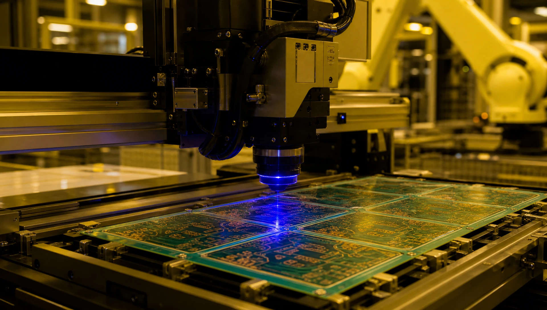
Submitting complete, production-ready Gerber and ODB++ datasets reduces engineering query (EQ) cycles and prevents production delays.
Mechanical Drill Aspect Ratio: Keep the aspect ratio (board thickness divided by drill diameter) at or below 10:1 for standard through-hole drilling (12:1 for advanced HDI builds) to guarantee reliable copper plating thickness inside via barrels.
Annular Ring Clearance: Provide a minimum outer annular ring width of 0.125 mm (5 mils) to prevent breakout during high-speed CNC drilling.
Trace-to-Board-Edge Distance: Maintain a minimum clearance of 0.30 mm (12 mils) between copper features and routed outer perimeters to avoid exposed copper burrs after panel singulation.
Solder Mask Dam Clearances: Maintain a minimum solder mask green dam width of 0.10 mm (4 mils) between adjacent SMT pads to eliminate solder bridging during automated reflow.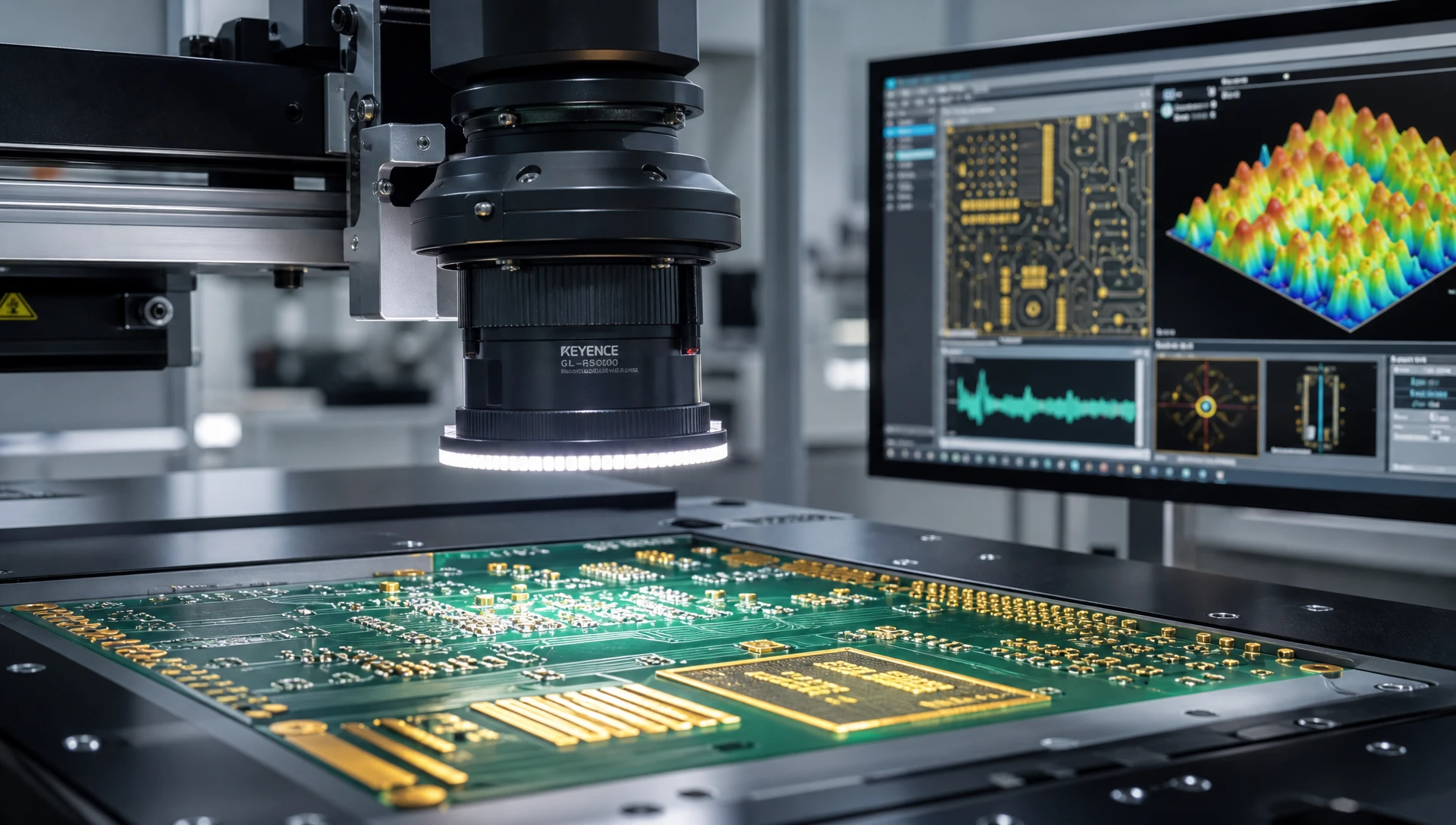
Mitigating international procurement risks requires clear communication protocols, transparent material sourcing, and structured logistics planning.
Approve Material Equivalence Upfront: Define approved alternate laminate foundries (e.g., Shengyi, Kingboard, Ventec, Isola) during early RFQ stages to avoid lead-time delays caused by local raw material shortages.
Establish Direct Engineering Communication: Partner with fabricators that provide direct access to English-speaking CAM (Computer-Aided Manufacturing) engineers to resolve engineering queries within 24 hours.
Implement Buffer Stock & Blanket Orders: For high-volume industrial lines, structure scheduled release orders with local buffer stock holding to shield production schedules from shipping delays.
To review processing capabilities, surface finish options, and layer stackups across single-sided, double-sided, and flex-rigid platforms, visit our full
Evaluating total cost of ownership (TCO) requires looking beyond initial unit costs to examine assembly labor, engineering support, freight logistics, and prototype agility.
| Evaluation Metric | Onshore Regional Fabricators | Certified China PCB Manufacturer | Strategic Procurement Impact |
| NPI Prototype Unit Cost | High ($300 - $800+ base rate) | Low-to-Moderate ($50 - $150 base rate) | Enables frequent iterative design testing within fixed R&D budgets. |
| Mass Production Scalability | Moderate (Capacity constraints) | High (Rapidly scalable volume) | Allows overseas brands to scale production rapidly to meet demand surges. |
| Tooling & Setup Charges | High NRE & NRE tooling fees | Competitive / Waived on volume | Lowers initial NPI barriers and ongoing production setup costs. |
| Turnaround Time (Standard) | 5 to 10 Business Days | 3 to 7 Business Days + Air Freight | Achieves comparable door-to-door delivery timelines via express air cargo. |
| Turnkey PCBA Integration | Higher assembly labor rates | Cost-effective turnkey SMT | Single-source accountability lowers total landed product costs. |
To examine our dedicated flexible circuit manufacturing lines and automated panel processing systems, explore our full
Navigating global supply chains requires an experienced, quality-driven production partner. As a leading china pcb manufacturer, ApolloPCB provides complete turn-key solutions for industrial automation, automotive, medical, and telecommunications OEMs worldwide.
Our modern manufacturing facilities feature high-speed LDI exposure systems, automated optical inspection lines, flying probe testers, and multi-layer vacuum lamination presses. From quick-turn prototypes to high-volume production, ApolloPCB guarantees IPC Class 2 and Class 3 compliance across every batch.
We offer full DFM analysis, custom stackup engineering, controlled impedance verification, and flexible delivery schedules to keep your production lines running smoothly.
Streamline your supply chain, lower manufacturing costs, and ensure long-term product reliability. Contact our engineering team today to submit your design files.
ApolloPCB enforces strict quality management frameworks including ISO 9001:2015 and IATF 16949 standards. Every production panel undergoes 100% Laser Direct Imaging (LDI), 3D Automated Optical Inspection (AOI), and electrical flying probe or bed-of-nails testing to guarantee zero-defect delivery.
ApolloPCB offers quick-turn prototype turnaround times as fast as 24 to 48 hours for standard double-sided boards, and 3 to 5 business days for complex multi-layer or flexible PCB builds, supported by express international air freight options.
Yes. ApolloPCB provides end-to-end solutions including bare PCB fabrication, authorized component procurement through official OCM channels, high-speed SMT placement, automated X-ray inspection (AXI), and functional circuit testing.

Got project ready to assembly? Contact us: info@apollopcb.com



 Whatsapp 0086 755 29438407
 Mail info@apollopcb.com
 Tel 0086 755 29438407


ABOUT US

PRODUCTS
TECHNOLOGY
KNOWLEDGE CENTRE
CULTURE
NEWS
We're not around but we still want to hear from you! Leave us a note:

Leave Message to APOLLOPCB
