




-
- PCB TYPE
- PRINTED CIRCUIT BOARD PROTOTYPE ALUMINUM PRINTED CIRCUIT BOARD R&F PCB FPC HIGH FREQUENCY PCB HIGH-TG PCB HEAVY COPPER PCB HDI PCB PCB FOR LIGHTING METAL CORE PCB


time:Jul 14. 2026, 21:15:09
Selecting the right LED package is one of the most critical decisions in modern hardware engineering. For Original Equipment Manufacturers (OEMs) and contract manufacturers, the choice goes far beyond aesthetics. It directly impacts your Printed Circuit Board (PCB) thermal management, assembly yield, power efficiency, and overall manufacturing cost.
If you are sourcing components or designing high-density layouts, understanding the nuances of smd led sizes is the first step toward building a reliable product. This comprehensive engineering guide breaks down the industry-standard dimensions, thermal characteristics, and strategic selection metrics that global electronics factories rely on.0
In surface mount technology (SMT), Surface Mount Device (SMD) LEDs are designated by four-digit codes. These numbers represent the physical length and width of the component package.
Depending on your region and your component supplier, these dimensions can be expressed in either the Imperial system (inches) or the Metric system (millimeters).
Misinterpreting imperial and metric codes is a frequent source of PCB assembly errors. For example, a 0603 imperial package is entirely different from a 0603 metric package:
Imperial 0603: Measures approximately 0.06 x 0.03 inches (1.6 x 0.8 mm). This is a highly popular, compact footprint for signal indicators.
Metric 0603: Measures 0.6 x 0.3 mm (equivalent to the tiny imperial 0201 package). This size is generally reserved for ultra-high-density designs like smartphones or medical micro-wearables.
Engineering Rule of Thumb: Always verify the measurement unit on your supplier's datasheet. Standard high-power and mid-power lighting LEDs (such as 2835, 3528, 5050, and 5630) are almost universally referenced using metric smd led sizes in mm.
To help you optimize your component selection, we have compiled a master reference table of the most common smd led sizes used in modern industrial and consumer electronics.
| Imperial Code | Metric Code | Dimensions (L x W x H in mm) | Typical Current (mA) | Power Rating (W) | Primary Applications |
| 0402 | 1005 | 1.0 x 0.5 x 0.45 | 5 - 15 | 0.02 - 0.05 | Membrane switches, ultra-thin backlighting, micro-indicators |
| 0603 | 1608 | 1.6 x 0.8 x 0.8 | 10 - 20 | 0.04 - 0.06 | Consumer electronics, network routers, status indicators |
| 0805 | 2012 | 2.0 x 1.25 x 0.8 | 15 - 20 | 0.06 - 0.1 | Industrial control panels, automotive dash lighting |
| 1206 | 3216 | 3.2 x 1.6 x 1.1 | 20 - 30 | 0.08 - 0.15 | Power supply status, test equipment, legacy industrial designs |
| N/A | 3528 | 3.5 x 2.8 x 1.9 | 20 - 30 | 0.06 - 0.1 | LED light strips, decorative architectural lighting |
| N/A | 2835 | 2.8 x 3.5 x 0.8 | 60 - 150 | 0.2 - 0.5 | Retrofit bulbs, office panel lights, commercial T8 tubes |
| N/A | 5050 | 5.0 x 5.0 x 1.6 | 60 (3 x 20) | 0.2 - 0.5 | Multi-color RGB lighting, smart home devices, signage |
| N/A | 5630 | 5.6 x 3.0 x 0.9 | 100 - 150 | 0.3 - 0.5 | High-efficiency commercial fixtures, bay lighting |
For a highly detailed layout analysis of these packages, including pad pattern layouts and solder mask clearances, check out our comprehensive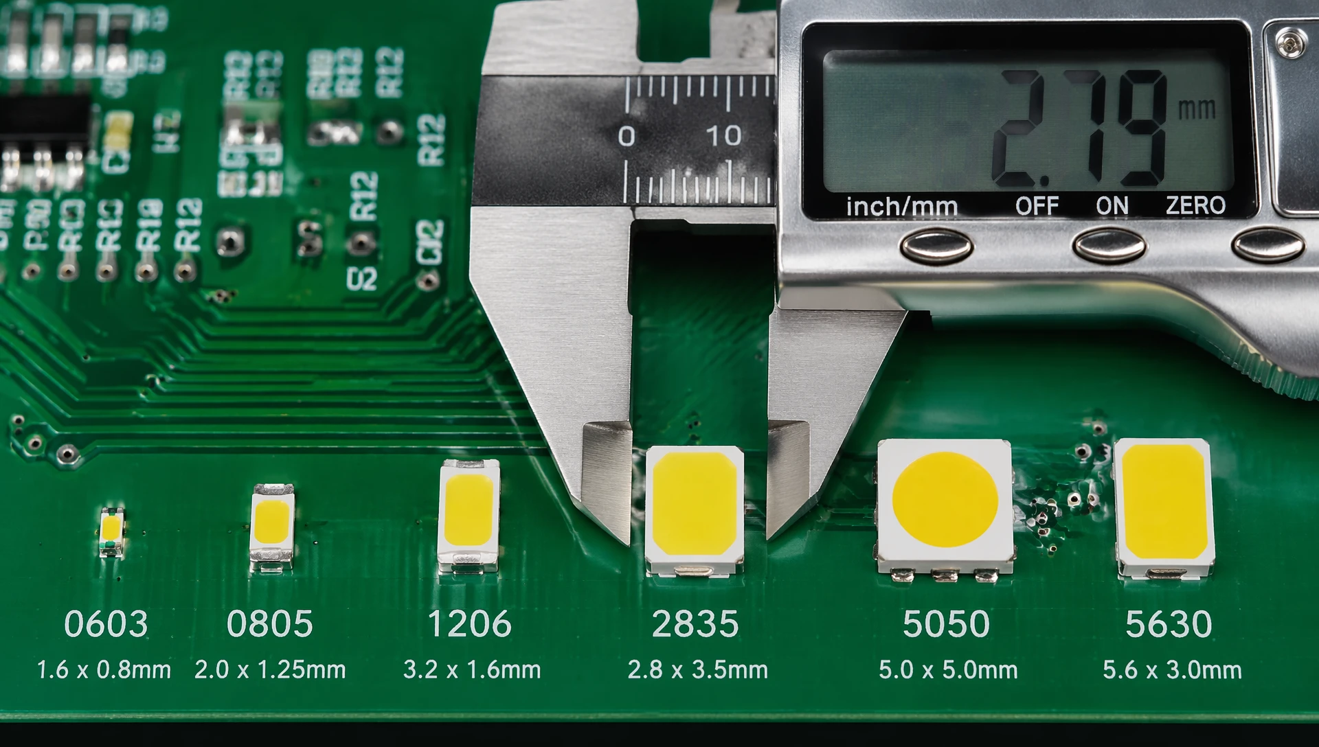
Let's look at the specific engineering profiles, thermal characteristics, and assembly considerations for the most popular SMD LED footprints in the global supply chain.
The Micro-Scale Champion: The 0402 is one of the smallest micro-LED footprints available.
Design Considerations: Because of its microscopic footprint, it is highly prone to tombstoning (a defect where the component stands vertically on one pad during reflow) if solder paste deposition or pad symmetry is even slightly off.
Best Used For: Extremely compact consumer electronics, smartwatches, and high-density interface panels where space is at a premium.
The Universal Indicator: The 0603 footprint balances space savings with ease of manufacturing.
Design Considerations: It is large enough to be easily placed by standard SMT pick-and-place machinery without specialized ultra-fine-pitch heads. It offers decent structural adhesion to the PCB.
Best Used For: Status indicators on power supplies, modems, medical monitors, and consumer appliances.
The Industrial Workhorses: These are larger, robust packages that provide excellent mechanical bonding and ease of visual inspection.
Design Considerations: They occupy more board real estate but are highly tolerant of manual prototyping, hand-soldering, and harsh, high-vibration environments.
Best Used For: Ruggedized automotive electronics, heavy industrial machinery controllers, and power conversion systems.
Though their length and width numbers are simply reversed, the 2835 and 3528 packages are engineered for completely different performance tiers:
3528 (Classic Low-Power): This older package features a relatively tall height (1.9 mm) and does not include an integrated thermal pad. It usually runs at low currents (20 mA) and is limited to accent lighting or decorative LED strips.
2835 (Modern High-Power): The 2835 is much thinner (0.8 mm) and features a massive integrated heat sink pad on its underside. This allows it to drive currents up to 150 mA or more, yielding far higher lumens per watt.
Supply Chain Impact: The 2835 has largely replaced the 3528 in general illumination due to its superior heat dissipation and lower material cost.
The Multi-Chip Pioneer: The 5050 package typically houses three separate LED chips (dies) within a single housing.
Design Considerations: Because it contains three chips, it can combine Red, Green, and Blue (RGB) dies to create millions of color variants, or run three white dies in parallel for high-brightness applications.
Best Used For: Smart home RGB/RGBW strip lighting, commercial signage, stage lighting, and automotive interior styling.
The High-Efficiency Luminaire: These packages are optimized for high lumen density.
Design Considerations: They feature a wider, elongated profile that distributes heat over a larger surface area. Designing for 5630 LEDs requires rigorous thermal simulation and often demands the use of Metal Core PCBs (MCPCBs) or thick copper ground planes to prevent lumen depreciation.
Best Used For: High-bay commercial lighting, streetlights, office troffers, and industrial searchlights.
When manufacturing at scale, selecting your LED package requires balancing physical constraints with thermal and structural reliability. Keep these primary design-for-manufacturability (DFM) variables in mind:
LEDs convert roughly 70% to 80% of their electrical power into heat rather than light. If the junction temperature of the LED exceeds its maximum rating, you will face rapid lumen depreciation, color shifting, and premature component failure.
For Low-Power LEDs (0402 - 1206): Standard FR4 PCBs with standard copper weights (1 oz/ft2) are generally sufficient.
For High-Power LEDs (2835, 5050, 5630): You must implement thermal vias directly under the LED thermal pad or transition to an aluminum-core Metal Core PCB (MCPCB).
To compare thermal pad configurations and reference physical footprints, check out our guide on
Your choice of SMD LED size dictates the manufacturing tolerances required of your PCBA partner:
Placement Accuracy: Ultra-small components like 0402 require high-speed, modern pick-and-place equipment with vision alignment.
Solder Paste Stencil Design: Stencil thickness and aperture design must be highly precise. An oversized aperture on a 0603 pad can lead to solder bridging, while an undersized aperture can lead to weak, dry solder joints.
Reflow Profile: High-power packages (like 5050) have high thermal mass. Your assembly partner must calibrate their reflow ovens with a profile that ensures the solder under the large central thermal pads melts completely without overheating the delicate LED lenses.
To prevent supply chain bottlenecks and minimize assembly defect rates, always design your PCB with standard, easily sourced footprints.
Whether you need a high-density FR4 indicator panel or a high-power aluminum-clad LED board, ApolloPCB is here to support you. We provide turn-key PCB fabrication and high-precision SMT assembly tailored to the strict quality standards that modern factories demand.
Ready to secure high-yield, high-reliability assembly for your next LED project?
Yes. We maintain an up-to-date smd led sizes chart pdf technical datasheet containing precise pad dimensions, mechanical drawings, and thermal pad layouts. Please visit our main resource hub or contact our support team directly to receive the latest copy of our engineering layout charts.
At ApolloPCB, we advise factory clients to phase out older 3528 footprints in favor of 2835 components. The 2835 package features a significantly larger integrated thermal pad and a lower profile. This design allows for up to three times better heat dissipation, permitting higher drive currents and superior long-term lumen maintenance.
The most common SMT defect with 0402 components is "tombstoning," which is caused by unbalanced surface tension in molten solder during reflow. ApolloPCB's manufacturing team prevents this by utilizing high-precision laser-cut stencils, optimizing copper trace symmetry under both pads, and strictly calibrating our pick-and-place nozzle positioning down to the micron level.

Got project ready to assembly? Contact us: info@apollopcb.com



 Whatsapp 0086 755 29438407
 Mail info@apollopcb.com
 Tel 0086 755 29438407


ABOUT US

PRODUCTS
TECHNOLOGY
KNOWLEDGE CENTRE
CULTURE
NEWS
We're not around but we still want to hear from you! Leave us a note:

Leave Message to APOLLOPCB
