-
- PCB TYPE
- PRINTED CIRCUIT BOARD PROTOTYPE ALUMINUM PRINTED CIRCUIT BOARD R&F PCB FPC HIGH FREQUENCY PCB HIGH-TG PCB HEAVY COPPER PCB HDI PCB PCB FOR LIGHTING METAL CORE PCB

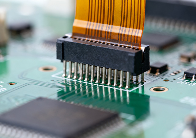
As high-end electronic devices evolve toward miniaturization, intelligence, and high performance, the demand for Precision Component FPC Assembly Service has surged dramatically. This specialized service focuses on the accurate assembly of micro-sized, high-precision components—such as microcontrollers, precision sensors, and ultra-small passive components—onto flexible printed circuits (FPCs). Unlike standard FPC assembly, which prioritizes basic connectivity, Precision Component FPC Assembly Service requires rigorous control over component placement accuracy, solder joint integrity, and FPC substrate stability to ensure optimal performance of high-end devices. For industries including precision medical equipment, aerospace electronics, and premium consumer gadgets, this service is a critical cornerstone for translating innovative designs into reliable, market-ready products.
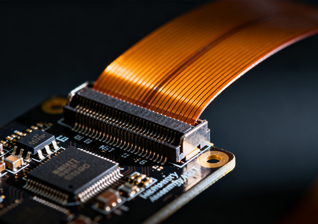
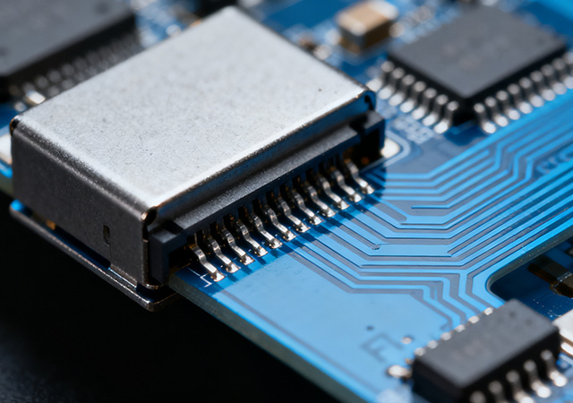
As electronic devices trend toward ultra-miniaturization, high functionality, and flexible form factors, High Density SMT FPC Assembly has emerged as a critical technology in advanced electronic manufacturing. This specialized assembly process combines the precision of high-density surface mount technology (SMT) with the flexibility of flexible printed circuits (FPCs), enabling the integration of hundreds of tiny components—such as microchips, resistors, and capacitors—onto flexible substrates. Unlike traditional rigid PCB SMT assembly, High Density SMT FPC Assembly requires unique expertise in handling flexible materials, controlling thermal stress, and ensuring precise component placement. For industries ranging from consumer electronics to medical devices and automotive systems, this assembly technology is a key enabler of products that balance compact design, high performance, and mechanical adaptability.
The global electronics industry’s shift toward flexibility, miniaturization, and intelligent integration has elevated the status of professional FPC manufacturers from mere component suppliers to strategic innovation partners. An FPC manufacturer specializes in the research, development, and production of flexible printed circuits (FPCs)—versatile components that enable seamless integration of electronic functions in constrained, curved, or dynamic environments. Unlike rigid PCB manufacturers, FPC manufacturers possess unique expertise in balancing mechanical flexibility with electrical performance, catering to the diverse needs of industries ranging from consumer electronics to industrial automation. For enterprises aiming to develop cutting-edge electronic products, partnering with a reputable FPC manufacturer is essential to translating design concepts into reliable, market-ready solutions.
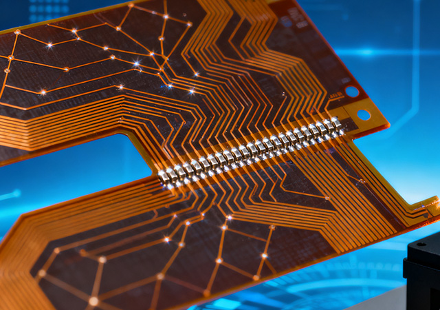
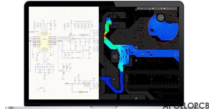
Expert HDI FPC manufacturer specializing in multilayer flex PCBs with microvias, blind/buried vias, and 0.05mm fine pitch. ISO9001 certified. Get a free DFM review and high-precision FPC quote today!
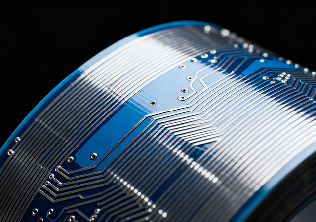
With the rapid evolution of electronic devices toward ultra-compact sizes, high-frequency operation, and multi-functional integration, the demand for high density interconnect (HDI) flexible printed circuits (FPCs) has become increasingly prominent. A professional High Density Interconnect FPC Producer serves as a core innovator in this field, specializing in the R&D and production of HDI FPCs that feature ultra-fine traces, micro vias, and advanced cross-layer interconnect structures. Unlike conventional FPC producers, these specialized providers possess in-depth expertise in resolving signal integrity issues, optimizing interconnect density, and adapting to diverse high-end application requirements. For brands engaged in 5G communications, autonomous driving, and precision medical devices, partnering with a reputable High Density Interconnect FPC Producer is crucial to realizing product innovation and maintaining market competitiveness.

Got project ready to assembly? Contact us: info@apollopcb.com


 Whatsapp 0086 755 29438407
 Mail info@apollopcb.com
 Tel 0086 755 29438407


ABOUT US

PRODUCTS
TECHNOLOGY
KNOWLEDGE CENTRE
CULTURE
NEWS
We're not around but we still want to hear from you! Leave us a note:

Leave Message to APOLLOPCB