




-
- PCB TYPE
- PRINTED CIRCUIT BOARD PROTOTYPE ALUMINUM PRINTED CIRCUIT BOARD R&F PCB FPC HIGH FREQUENCY PCB HIGH-TG PCB HEAVY COPPER PCB HDI PCB PCB FOR LIGHTING METAL CORE PCB


time:May 27. 2026, 10:12:06
In the hyper-competitive global hardware market, speed and scalability are no longer just operational goals—they are baseline requirements for survival. For hardware entrepreneurs, product development managers, and global procurement heads, the path from a conceptual napkin sketch to a market-ready, high-volume hardware product is fraught with hidden risks. This is particularly true when dealing with advanced flexible printed circuits (FPCs), where spatial constraints, multi-axial bending, and high-density connectivity require flawless execution.
The primary bottleneck for global B2B procurement teams typically lies in vendor fragmentation. Hardware engineering teams often utilize small, specialized quick-turn prototype shops to test early iterations, only to face severe logistical, mechanical, and pricing friction when trying to migrate that design to a massive Original Equipment Manufacturer (OEM) assembly facility.
To overcome this structural barrier, leading enterprises are turning to integrated manufacturing partners capable of consolidating the entire hardware lifecycle under a single operational umbrella. As an agile, technology-driven FPC manufacturer, ApolloPCB bridges this gap, providing accelerated prototyping engineering and high-yield, large-scale OEM scaling solutions.
By executing exhaustive Design for Manufacturing (DFM) checkouts during the initial sampling phase, we deliver premium advanced flexible PCB solutions that reduce time-to-market and ensure long-term product viability.
When technology companies introduce new products via the New Product Introduction (NPI) framework, procurement managers face a persistent dilemma. Early-stage hardware development demands a fast-turn FPC manufacturer that can deliver functional engineering samples within days. However, those prototype-focused facilities rarely possess the automated roll-to-roll (R2R) production assets, strict IATF 16949 credentials, or massive supply chain leverages necessary to handle high-volume commercial production.
This vendor disconnect introduces severe operational vulnerabilities to your business:
Engineering Translation Errors: A design optimized for a low-volume prototype shop’s manual processing lines often fails miserably when fed into a highly automated OEM assembly line. Trace geometries, pad dimensions, and coverlay registration targets must be re-engineered, causing unexpected delays.
Compounded Certification Costs: Switching from a prototype vendor to a high-volume factory requires a complete repetition of quality audits, first-article inspections (FAI), and functional environmental testing.
Fragmented Accountability: If a post-assembly defect arises, the prototype developer, the bare-board supplier, and the final SMT assembler often point fingers at each other, leaving the client with expensive, unsalvaged scrap.
ApolloPCB eliminates this friction by operating a dual-pipeline facility. Our quick-turn prototyping division interfaces seamlessly with our advanced mass-production floors. This unified workflow guarantees that every engineering insight gained during a 3-day prototype run is automatically embedded into the high-volume tooling matrix, maintaining absolute continuity from the initial revision to million-unit monthly rollouts. For a detailed review of our foundational technical spectrum, explore our benchmark article on custom FPC and HDI flexible PCB solutions.
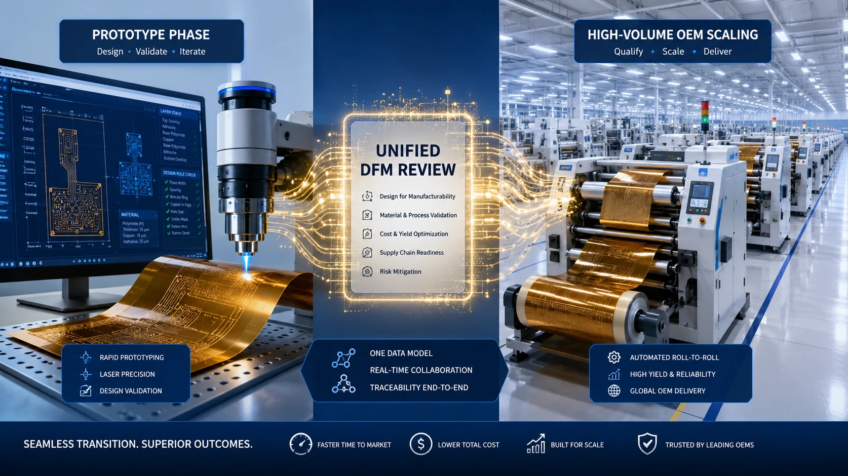
A successful FPC prototype rollout is about more than just fast manufacturing turnaround times; it is about proactive risk management. Flexible circuits are fundamentally active mechanical elements that undergo repetitive physical stress. If engineering anomalies are not caught during the digital simulation phase, they will lead to trace fractures, delamination, and component tear-offs in the field.
When B2B clients partner with a premier customize FPC manufacturer like ApolloPCB, their design files undergo an intensive, automated Design for Manufacturing (DFM) and Design for Assembly (DFA) audit prior to panellization. Our dedicated engineering cells analyze your specific application layer to neutralize common layout mistakes before they impact your financial budget.
To help supply chain managers understand how engineering parameters shift across the product life cycle, the following matrix outlines the strategic operational parameters utilized on our production floor:
| Operational Parameter | Quick Prototype Phase | Full-Scale OEM Phase | Client Value & Deliverables |
| Standard Lead Times | 3 to 5 Business Days | 12 to 18 Business Days | Compresses R&D loops; enables rapid market validation. |
| Tooling Method | Laser Direct Imaging (LDI) & Laser Cutting | Hard Punching Dies & Matrix Photolithography | Eliminates setup costs early on; guarantees structural uniformity at scale. |
| Panelization Strategy | Specialized Matrix Nesting | High-Density Roll-to-Roll (R2R) Optimization | Maximizes raw material utilization to lower per-piece costs. |
| Trace & Space Tolerance | Down to 35μm | Down to 25μm | Supports high-density component scaling as designs mature. |
| 100% Quality Validation | Flying Probe Testing & Digital AOI | Dedicated Bed-of-Nails Fixtures & 3D Automated Inspection | Secures zero-defect field reliability across millions of shipped units. |
Our engineering interventions focus heavily on structural longevity. For example, if a client submits an FPC design with sharp 90-degree corners in the bend zone, our engineers will automatically modify them to smooth, radiused curves to distribute mechanical stress evenly.
Furthermore, we ensure that solid copper ground planes are converted into hatched copper configurations within dynamic flexing areas. This structural change significantly improves flexibility, reduces board stiffness, and prevents copper work-hardening over thousands of bend cycles, aligning with the stringent parameters required for high-flex automotive FPC performance .
As consumer products, wearables, and high-frequency communication modules continue to contract in physical size, the density of surface-mount components escalates exponentially. To meet these spatial demands, modern OEM products require specialized flexible board architectures that surpass standard single- or double-sided layouts.
ApolloPCB addresses these high-density requirements by acting as an elite, high-volume HDI FPC manufacturer. We support complex multi-layer configurations (up to 8 layers of pure polyimide film) featuring advanced sub-100μm blind and buried microvia arrays.
[Raw Engineering CAD] -> Precise DFM Optimization -> Laser Direct Imaging (LDI)
                                                               │
                                                               ▼
[High-Density Assembly] <- ENEPIG Surface Finishing <- Microvia Laser Drilling
                                                               │
                                                               ▼
[Automated 3D AOI Checkout] -> 100% Flying Probe Test -> Final OEM Product Delivery
Operating as a reliable blind and buried vias FPC manufacturer, we employ advanced ultraviolet (UV) laser ablation assets alongside periodic-reverse pulse copper plating. This setup allows our factory floor to drill and cleanly fill microvias down to 50μm in diameter, enabling via-in-pad structures that save vital board real estate.
To support the fine-pitch SMT requirements of advanced micro-processors, we deploy Electroless Nickel Electroless Palladium Immersion Gold (ENEPIG) surface finishes. This ultra-flat surface prevents component tilting during assembly and serves as an exceptional foundation for FPC gold ball bonding, ensuring robust wire-bond connections between semiconductor components and the flexible copper tracks. These high-tier manufacturing processes are detailed in our factory capability overview on advanced multi-layer FPC factory manufacturing capabilities.
A reliable manufacturing partner must be highly versatile, capable of adapting its lines to satisfy the unique compliance standards and material requirements of diverse vertical market sectors. ApolloPCB maintains distinct production modules optimized for specific commercial applications:
In the fast-moving mobile arena, we function as a strategic smartphone FPC manufacturer and Dsiplay FPC manufacturer. These components demand trace and space dimensions down to 25μm to accommodate high-definition MIPI, display, and camera signals within cramped mechanical hinges. Our roll-to-roll (R2R) lamination lines ensure precise layer-to-layer registration across long production runs, preventing signal degradation and guaranteeing perfect display refresh rates for end consumers.
For industrial machinery, control enclosures, and smart appliances, our infrastructure functions as an agile KeyPads FPC manufacturer and LED Lighting FPC manufacturer. Keypad applications require integrated carbon or gold-plated contact pads that withstand millions of mechanical tactile activations.
Meanwhile, our lighting and linear sensor lines are capable of processing continuous flexible circuits exceeding 5 meters in length without cumulative registration drift, providing the thermal dissipation required to prevent LED heat accumulation.
To support the rapidly expanding green energy sector, our lines function as an authoritative Batteries FPC manufacturer. Electric vehicle battery packs and large energy storage arrays rely on long, multi-layer flexible harnesses to monitor cell temperatures and individual voltages in real time.
ApolloPCB etches heavy copper foils (up to 3 oz) onto high-TG polyimide bases. This allows these critical safety components to carry cell-balancing currents without overheating, stripping away kilograms of vehicle weight compared to traditional, hand-wired copper wire harnesses.
The ultimate goal for modern procurement leads is to source a completely finalized sub-assembly from a single vendor. Sourcing bare flexible sheets from one manufacturer and shipping them to a third-party Electronic Manufacturing Services (EMS) provider introduces severe handling and quality tracking risks. Flexible substrates are fragile; improper handling can micro-fracture internal traces or warp pads before components are placed.
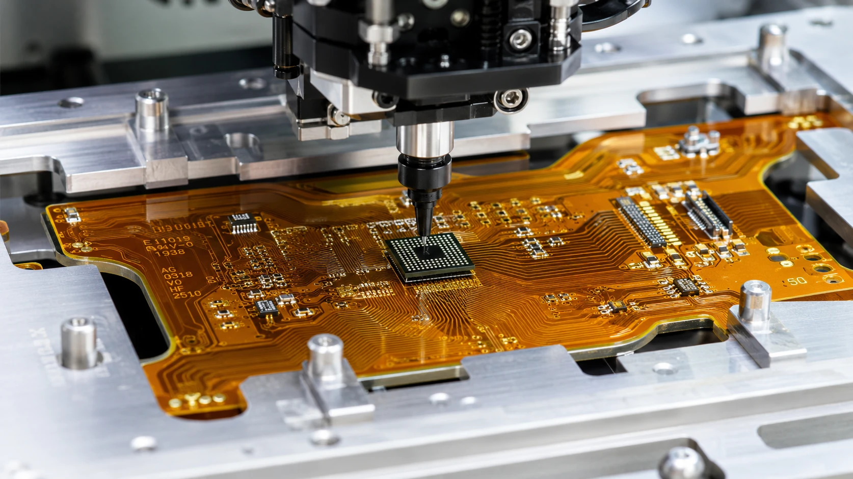
To protect our clients' investments, ApolloPCB provides fully integrated FPC High Density Component Assembly services within our cleanroom SMT environments. We control the entire component attachment workflow through custom-engineered tooling and strict process discipline:
Precision Carrier Fixturing: Every flexible circuit panel is locked onto custom-milled, rigid aluminum or magnetic vacuum plates. This keeps the polyimide film flat during high-speed pick-and-place routines and prevents solder paste distortion.
Pre-Assembly Vacuum Dehydration: Because polyimide is highly hydroscopic and absorbs ambient moisture, all FPC panels undergo mandatory vacuum baking cycles prior to entering reflow ovens. This completely eliminates internal moisture, preventing outgassing, delamination, or blistering at lead-free reflow temperatures (260°C).
Automated Structural Reinforcement: We integrate localized FR4, polyimide, or aluminum stiffeners using precise thermosetting or pressure-sensitive adhesives (PSA) underneath high-pin-count connectors, ensuring the FPC easily withstands mechanical insertion forces during final product assembly.
Every completed batch is backed by 100% automated optical inspection (AOI), X-ray checking for BGA packages, and rigorous functional testing, providing global procurement teams with an authoritative layer of operational trust and manufacturing confidence.
A1: We utilize the exact same engineering data matrix, CAM software, and core chemical processing parameters for both our prototyping and mass-production lines. The DFM parameters verified during your prototype run are preserved, meaning your design can be scaled up to high-volume hard-tooling lines instantly without requiring a complete re-engineering phase.
A2: We offer FR4, Polyimide (PI), and stainless steel/aluminum stiffeners. FR4 is typically selected beneath heavy SMT components to provide rigid structural support. Polyimide stiffeners are utilized to increase the thickness of insertion fingers (such as ZIF connectors) to meet exact mating specifications. Stainless steel and aluminum are applied in high-stress or high-thermal environments where exceptional mechanical rigidity or grounding is required.
A3: Polyimide films naturally absorb ambient atmospheric moisture over time. If a flexible circuit is subjected to lead-free reflow profiles (260°C) without pre-baking, this trapped moisture vaporizes instantly, causing internal micro-explosions that delamination inner layers or fracture microvias. Our strict vacuum-baking protocol completely dehydrates the FPC substrate, ensuring zero-defect assembly yields.
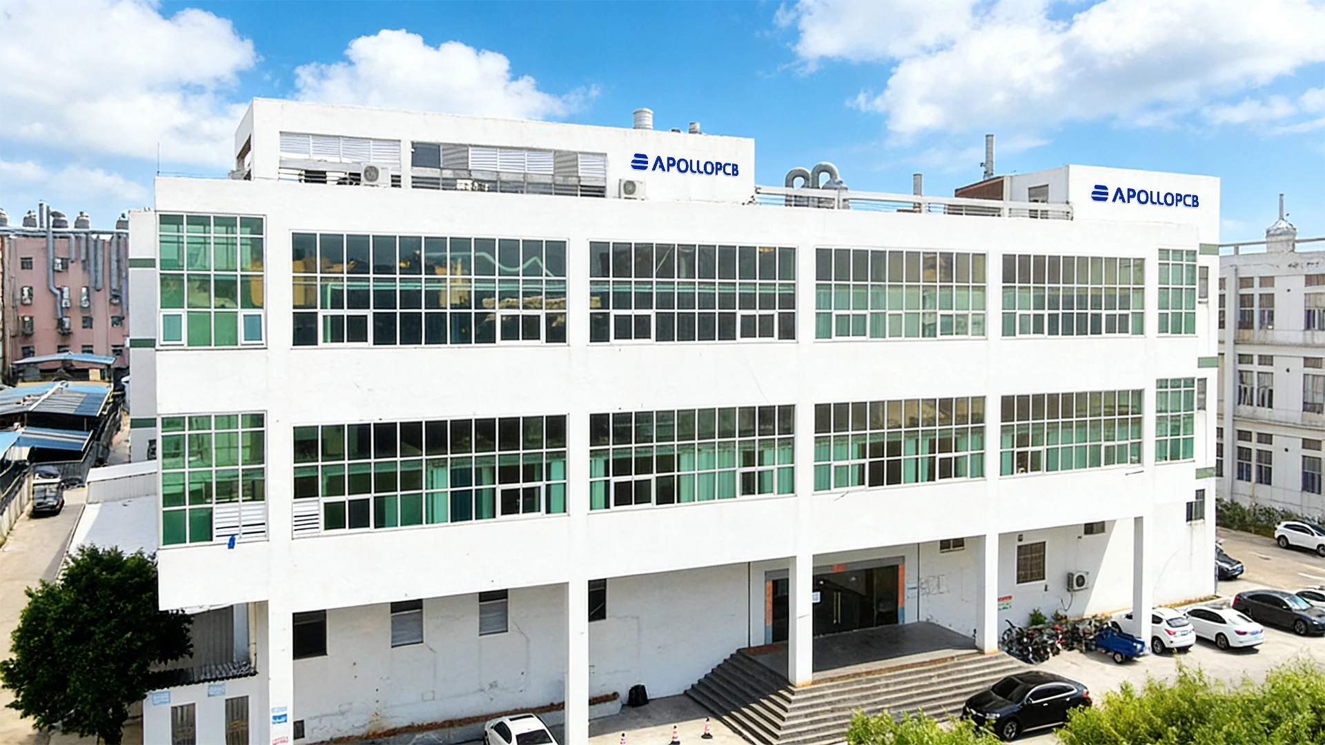
Navigating a product launch requires a manufacturing partner that can move seamlessly between fluid R&D iterations and highly structured, high-volume production. ApolloPCB blends the responsiveness of a quick-turn prototype shop with the manufacturing scale, quality controls, and financial stability of an established OEM manufacturer.
From implementing precision blind and buried vias FPC manufacturer techniques to handling high-volume smartphone FPC manufacturer rollouts, we engineer cost-efficiency, yield control, and structural durability into every custom project. Let us help you eliminate vendor fragmentation, reduce hidden logistics overhead, and compress your product development timeline.
Ready to accelerate your product development loop and secure your high-volume OEM pipeline? Request a custom FPC technical quote from the ApolloPCB engineering team today, and discover how our integrated prototype-to-production solutions can drive value for your business.
Custom FPC Manufacturer: HDI & Flexible PCB Solutions | ApolloPCB
Smartphone FPC Manufacturer | High-Density HDI & Multi-layer Flex PCB
Durable Keypad FPC Manufacturer: High-Cycle & Reliable Flex Solutions

Got project ready to assembly? Contact us: info@apollopcb.com



 Whatsapp 0086 755 29438407
 Mail info@apollopcb.com
 Tel 0086 755 29438407


ABOUT US

PRODUCTS
TECHNOLOGY
KNOWLEDGE CENTRE
CULTURE
NEWS
We're not around but we still want to hear from you! Leave us a note:

Leave Message to APOLLOPCB
