-
- PCB TYPE
- PRINTED CIRCUIT BOARD PROTOTYPE ALUMINUM PRINTED CIRCUIT BOARD R&F PCB FPC HIGH FREQUENCY PCB HIGH-TG PCB HEAVY COPPER PCB HDI PCB PCB FOR LIGHTING METAL CORE PCB
Real PCB &PCB Assembly Manufacturer
IS09001:2015 Standard
UL.RoHS. REACH Certified
3000+ Orders/Day
99% on-time Shipping
100,000+ Customers
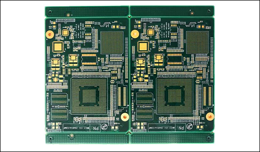
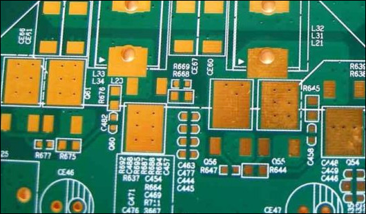
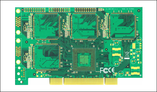
HDI PCB is the high-density interconnector PCB. It is a type of PCB technology that is very popular in various devices. HDI PCBs are the results of miniaturization of components and semiconductor packages because they can realize more functions on the same or less board area through some technologies.

The characteristics of HDI PCBs in designing and manufacturing
HDI PCBs have finer lines, minor holes, and higher density than conventional PCBs, providing necessary touting solutions for the chips with many pins in mobile devices and other high-tech products.
undefined
HDI design combines dense component placement and finer circuits, using less board without compromise functions. Compared to ordinary PCBs, the main difference is that HDI PCBs realize the interconnect through blind vias and buried vias instead of through holes. And HDI PCBs use laser drilling while traditional PCBs usually use mechanical drilling. Laser drilling allows smaller apertures whose sizes are in the range of 3.0-6.0mil, which will save much space of the pad, and more layout can be achieved in the unit area.

The advantages and applications of HDI PCBs
· Compact design
The combination of micro vias, blind vias, and buried vias reduces the board space greatly. With the support of HDI technologies, a standard 8-layers through-hole PCB can be simplified to a 4-layer HDI PCB with the same functions.
· Excellent signal integrity
With small vias, all stray capacitance and inductance will get reduced. And the technology of incorporating bind vias and via-in-pad helps to shorten the length of the signal path. These will lead to faster signal transmission and better signal quality.
· High reliability
HDI technology makes route and connect easier, and offers PCBs better durability and reliability in hazardous conditions and extreme environment.
· Cost-effective
There needs much more manufacturing cost when the boards are beyond 8-layer if using traditional pressing processes. But HDI technology can reduce the cost and keep the function purpose.
HDI PCBs have been used widely to reduce the entire size and weight of final products while enhancing the electrical performance. For these medical devices like pacemakers, miniaturized cameras, and implants, only HDI techniques are capable of supplying small packages with fast transmission rates. HDI PCBs are responsible for smaller portable products, such as smartphones, tablets, and wearable electronics. Automotive devices, military, and aerospace equipment also need the support of HDI technologies.

The birth of the HDI PCBs brings more possibilities for portable electronic devices and more challenges for PCB manufacturers. For accommodating the trend of miniaturization and multifunction of electronics, APOLLOPCB has done a lot to improve the level of equipment and staff professionalism. You can be assured to offer us the HDI designs, and we will give you a satisfactory service and HDI products

Got project ready to assembly? Contact us: info@apollopcb.com


We're not around but we still want to hear from you! Leave us a note:

Leave Message to APOLLOPCB
