-
- PCB TYPE
- PRINTED CIRCUIT BOARD PROTOTYPE ALUMINUM PRINTED CIRCUIT BOARD R&F PCB FPC HIGH FREQUENCY PCB HIGH-TG PCB HEAVY COPPER PCB HDI PCB PCB FOR LIGHTING METAL CORE PCB
time:Jan 12. 2026, 13:15:36
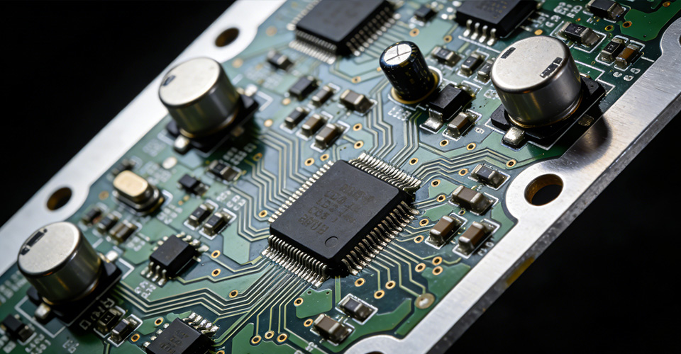
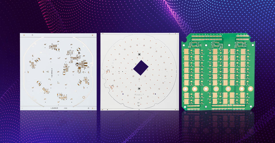
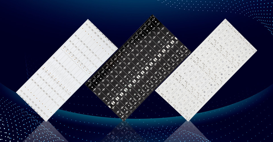
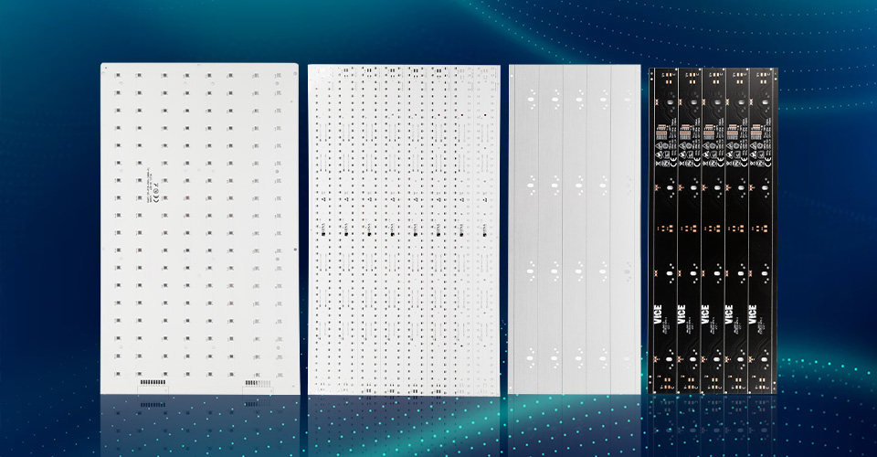
If you’re sourcing an aluminum pcb for high-power LED lighting or power electronics, the real success metric isn’t “cheap per panel”—it’s thermal performance, flatness during assembly, stable quality control, and lead-time reliability. Metal-core PCBs (MCPCB / IMS) are built to move heat away from hotspots far more effectively than standard FR-4, making them a common choice in LED lighting and power supplies where heat is a major factor.
This article is written for factory buyers and engineers evaluating an aluminum pcb manufacturer (including aluminum pcb china sourcing), and it also covers advanced routing options such as blind and buried vias aluminum pcb for compact, high-density designs.
An aluminum substrate pcb (often called aluminum pcb or MCPCB) typically uses a three-layer stack:
Circuit layer (copper foil)
Thermally conductive dielectric layer
Base layer (aluminum)
This structure creates a direct heat path from components through the dielectric into the metal base, helping reduce junction temperature and improving long-term reliability.

Aluminum MCPCBs are widely used in LED lighting because controlling junction temperature directly impacts lumen maintenance and service life. For outdoor light PCB projects, the board must survive high ambient temperatures, sealed housings, and long duty cycles. In many production cases, aluminum MCPCB helps reduce hotspot stress and supports longer service life.
Metal-base PCBs are frequently used in power electronics where heat is concentrated in MOSFETs/IGBTs, rectifiers, and current-sense networks. In compact layouts, thermal stability is often directly linked to efficiency, safety margins, and lifetime.

When comparing any aluminum pcb manufacturer, your RFQ should include the items below so you get accurate pricing and avoid schedule delays:
Target dielectric thermal conductivity (commonly 1W / 2W / 3W / 8W / 12W options)
Dielectric thickness preference (often discussed in ranges like 50–200μm)
Operating environment: ambient temperature, enclosure type, airflow, lifetime target
For aluminum pcb, warpage control is a common challenge due to material differences between copper, dielectric, and aluminum base. If you assemble high-power LEDs or large panels, ask your supplier about warpage control targets and inspection methods.
If you build power supplies or high-voltage LED drivers, specify isolation needs and testing requirements (e.g., withstand voltage test). This is a key factory qualification item for many aluminum substrate pcb projects.
Copper weight impacts current handling and heat spreading. For power electronics, specify copper weight, trace current targets, and expected temperature rise, so the supplier can confirm manufacturability.

If you’re searching aluminum pcb china suppliers, published capability limits help you qualify faster. A typical capability snapshot for metal-base PCBs can include:
Max layers (for some suppliers, up to 8 layers)
Max board thickness (e.g., around 4.0mm depending on process)
Max delivery panel size (large-format panels for lighting modules)
Copper weight capability (often up to 6oz on some lines)
Drilling limits on aluminum base (minimum and maximum drill sizes)
Breakdown voltage capability for isolation design
Thermal performance range (based on dielectric selection)
Supported metal base materials (aluminum, copper, etc.)
For factory procurement, capability tables should be checked against your exact stackup, hole sizes, and panelization needs.
An aluminum pcb may look simple, but yield depends on discipline in drilling, dielectric integrity, and final testing. Before mass production, ask the supplier to confirm:
Incoming material control and traceability (dielectric + aluminum base)
Drilling/milling control on metal base
Solder mask and surface finish consistency
Inspection coverage (AOI) and defect criteria
Electrical test method (flying probe / fixture test)
For assembled boards: X-ray inspection for voids/bridges when needed
Factories should request sample inspection evidence or reports when onboarding a new aluminum pcb manufacturer.

Most LED boards are single-layer or simple double-layer. But once you integrate compact drivers, high-density control, or mixed-signal sections, via strategy becomes a real lever.
Blind vias connect outer layers to inner layers without going through the entire board.
Buried vias connect inner layers only and are not visible from the surface.
For compact layouts, blind and buried vias aluminum pcb can improve routing density, reduce surface congestion, and shorten interconnect paths for better signal integrity. However, they also increase process complexity and cost, so they should be applied where they materially reduce PCB size or improve performance.
To quote fast and correctly, send:
Gerber + drill files
Stackup targets (dielectric thickness / thermal conductivity / copper weight)
Surface finish, solder mask requirements, outline/panel requirements
Quantity, target lead time, ship-to country
If assembly is needed: BOM + Pick&Place + assembly drawing
This package helps any aluminum pcb manufacturer respond quickly and reduces the risk of re-quotation.
A: An aluminum pcb uses a metal base with a thermally conductive dielectric and copper circuit layer. This improves heat spreading and reduces hotspot temperatures—ideal for LED and power electronics where heat impacts reliability.
A: No. Many lighting boards are single-layer, but aluminum substrate pcb can also be made as double-layer or multilayer (depending on supplier process), which supports better routing density and power distribution.
A: Ask for capability limits (panel size, copper weight, drilling range), quality controls (inspection + electrical test), and process control for warpage/flatness. These items strongly affect yield and long-term stability.
A: Outdoor light PCB applications operate in sealed housings and harsh environments for long periods. Aluminum MCPCB improves thermal performance, reduces LED stress, and supports longer service life in real-world outdoor conditions.
A: Yes. Blind and buried vias aluminum pcb helps increase routing density and reduces surface congestion for compact designs. Blind vias connect outer-to-inner layers; buried vias connect inner layers only. They cost more due to additional manufacturing steps, so they should be used when density or performance requires it.

Got project ready to assembly? Contact us: info@apollopcb.com


We're not around but we still want to hear from you! Leave us a note:

Leave Message to APOLLOPCB
