-
- PCB TYPE
- PRINTED CIRCUIT BOARD PROTOTYPE ALUMINUM PRINTED CIRCUIT BOARD R&F PCB FPC HIGH FREQUENCY PCB HIGH-TG PCB HEAVY COPPER PCB HDI PCB PCB FOR LIGHTING METAL CORE PCB
time:Nov 03. 2025, 11:54:21
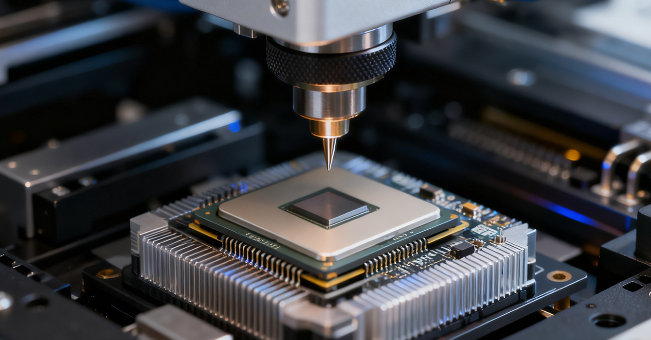
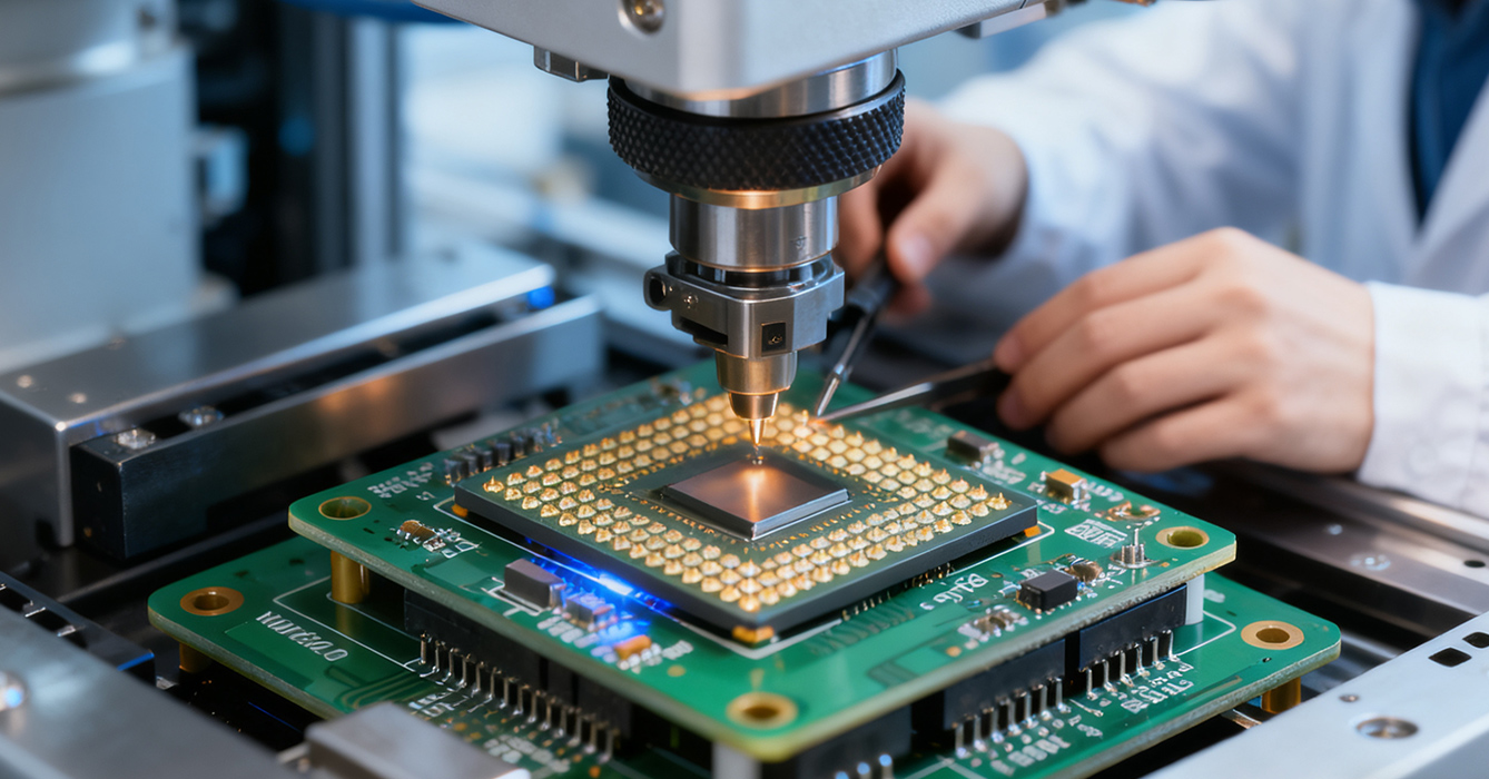
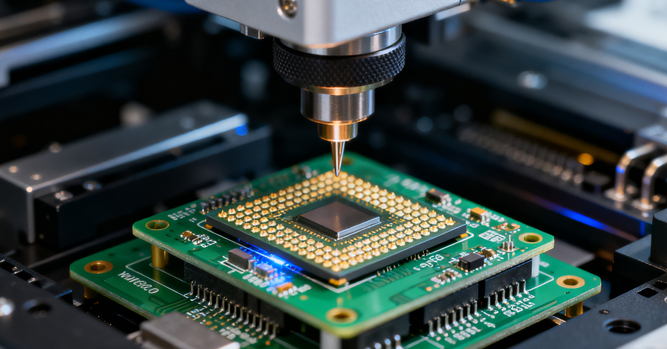
BGA Assembly for High-End Devices is a specialized discipline that bridges cutting-edge semiconductor design with the stringent performance demands of premium electronics. High-end devices—including flagship smartphones, AI-powered servers, ultra-high-definition medical imagers, and enterprise-grade networking equipment—require BGA (Ball Grid Array) assemblies that deliver uncompromised signal integrity, thermal resilience, and long-term reliability. Unlike standard consumer electronics, these devices operate under extreme conditions: high data throughput, continuous heavy loads, and often harsh environments (e.g., industrial heat or medical sterilization). As such, BGA assembly for high-end applications demands tailored processes, advanced materials, and rigorous quality control to unlock the full potential of next-generation semiconductors.

High-end devices impose three core challenges that define their BGA assembly requirements:
- Extreme Miniaturization with High I/O Density: Flagship smartphones and compact AI accelerators pack thousands of I/O connections into millimeter-scale chips. BGA assemblies must support ultra-fine pitches (down to 0.4mm) and micro-solder balls, requiring sub-micron placement accuracy to avoid bridging or open circuits.
- Thermal Management Under Heavy Loads: High-performance chips (e.g., 5G baseband processors or GPU clusters) generate significant heat. BGA assemblies must integrate thermal vias, heat spreaders, or even embedded cooling solutions to prevent solder joint degradation and ensure stable operation.
- Mission-Critical Reliability: Medical devices (e.g., MRI scanners) and aerospace electronics require BGA assemblies with zero failure tolerance. This demands resistance to thermal cycling, vibration, and chemical exposure—far exceeding the durability of standard consumer-grade assemblies.

To meet high I/O density needs, BGA assembly for high-end devices leverages heterogeneous integration techniques. This includes chip-on-chip (CoC) and system-in-package (SiP) designs, where multiple dies (e.g., processor, memory, and RF module) are stacked or side-by-side within a single BGA package. Precision underfill materials—with low thermal expansion coefficients—are used to reinforce solder joints, reducing stress from thermal cycling and ensuring long-term connectivity.
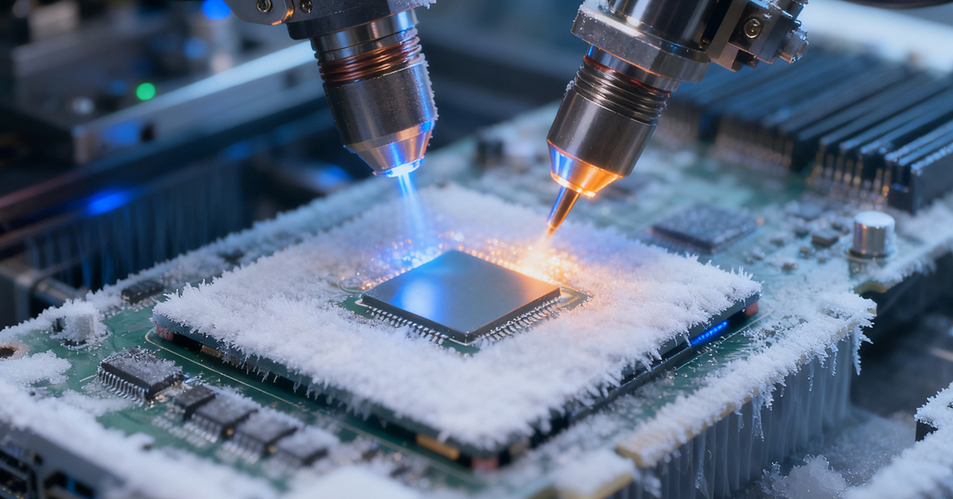
Thermal management starts during assembly. Reflow ovens with nitrogen atmosphere control minimize oxidation of solder joints, improving wetting and reducing voids (a major cause of heat-related failures). Additionally, selective soldering techniques target high-heat components, preventing damage to adjacent sensitive parts. Post-assembly, thermal interface materials (TIMs) with high thermal conductivity are applied between the BGA package and heat sinks, optimizing heat dissipation.
High-end BGA assemblies undergo more stringent testing than standard counterparts. This includes X-ray inspection with 3D tomography to detect hidden solder defects, thermal cycling tests (-40°C to 125°C for thousands of cycles), and vibration testing to simulate real-world operating conditions. For medical and aerospace applications, statistical process control (SPC) is implemented to ensure every assembly meets Six Sigma quality standards.

Premium smartphones use BGA assemblies for 5G millimeter wave modules, image signal processors (ISPs), and high-performance SoCs. Ultra-fine-pitch BGA (UFPBGA) enables thinner designs without sacrificing processing power, while underfill materials protect solder joints from drops and temperature fluctuations.
AI servers with GPU clusters rely on BGA assemblies that support high-speed data transfer (up to 112Gbps per lane). Advanced BGA designs with controlled impedance traces ensure signal integrity, while embedded heat pipes in the package dissipate heat from continuous AI model training.
CT scanners and MRI machines use BGA assemblies in their signal processing units. These assemblies are built with biocompatible materials and undergo sterilization-resistant treatments, ensuring reliability in clinical environments while maintaining the high data throughput needed for detailed imaging.

As high-end devices push toward 6G, quantum computing, and edge AI, BGA assembly will evolve further. Emerging trends include nanoscale solder interconnects for quantum chips, self-healing underfill materials that repair micro-cracks, and AI-driven predictive maintenance for assembly lines—ensuring zero defects in even the most complex high-end devices.
BGA Assembly for High-End Devices is a critical enabler of innovation in premium electronics, requiring a fusion of precision engineering, material science, and quality rigor. By addressing the unique demands of miniaturization, thermal management, and reliability, this specialized assembly process ensures high-end devices deliver the performance and durability that define their value. As technology advances, BGA assembly will remain at the forefront, unlocking new possibilities for the next generation of high-performance electronics.

Got project ready to assembly? Contact us: info@apollopcb.com


We're not around but we still want to hear from you! Leave us a note:

Leave Message to APOLLOPCB
