-
- PCB TYPE
- PRINTED CIRCUIT BOARD PROTOTYPE ALUMINUM PRINTED CIRCUIT BOARD R&F PCB FPC HIGH FREQUENCY PCB HIGH-TG PCB HEAVY COPPER PCB HDI PCB PCB FOR LIGHTING METAL CORE PCB
time:Jun 13. 2025, 12:48:40
In the rapidly evolving electronics industry, the demand for smaller, more powerful, and energy - efficient devices is driving continuous innovation in printed circuit board (PCB) technology. Metal - Core Printed Circuit Boards (MCPCBs) have become a staple in high - power applications due to their excellent thermal management capabilities, while High - Density Interconnect (HDI) designs enable the miniaturization of electronic components by increasing circuit density. The integration of blind and buried vias in MCPCBs for HDI designs represents a significant advancement, combining the benefits of both technologies to meet the stringent requirements of modern electronics. This article explores the role, design, manufacturing, and quality control of blind buried vias in MCPCB HDI designs, along with their applications, challenges, and future trends.
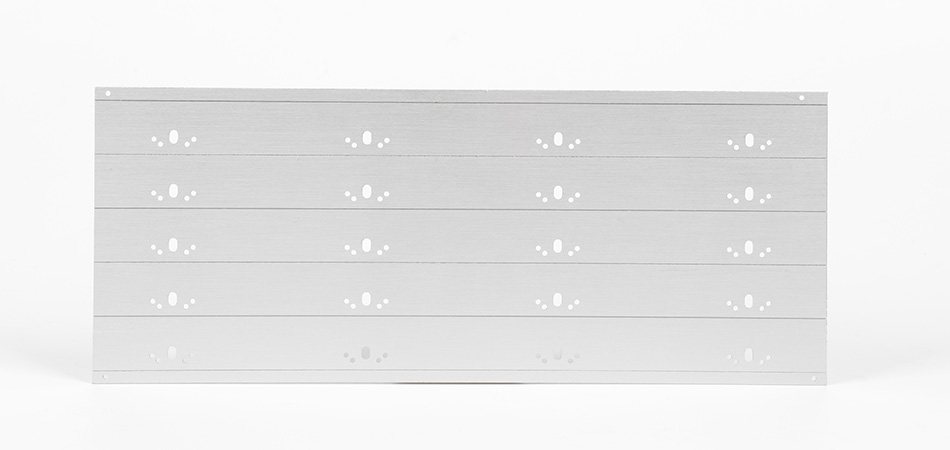
MCPCBs feature a three - layer structure: a metal core, usually made of aluminum or copper, which serves as an efficient heat sink; an insulating dielectric layer that electrically isolates the metal core while facilitating heat transfer; and a conductive layer, typically copper, with etched electrical traces. The metal core’s high thermal conductivity allows for effective heat dissipation in high - power applications, preventing component overheating and extending device lifespan.
HDI designs focus on increasing the density of components and electrical connections on a PCB. They utilize techniques such as smaller trace widths, finer pitch components, and advanced via structures to achieve higher functionality in a reduced space. HDI PCBs are crucial for modern electronics like smartphones, tablets, and high - end servers, where compactness and performance are key.
Vias are holes in a PCB that connect different layers electrically. Blind vias connect the outer layer to an inner layer, while buried vias connect two inner layers without reaching the surface. These vias save space by reducing the need for through - hole vias that penetrate the entire board, enabling more efficient use of the PCB surface area and enhancing electrical performance by minimizing signal interference.

In HDI designs, space is at a premium. Blind buried vias eliminate the need for through - hole vias that extend through the entire MCPCB, freeing up valuable surface area. This allows for a denser component layout, accommodating more electronic components within the same footprint. For example, in compact wearable devices, every millimeter of space saved can enable the addition of new features or a smaller form factor.
Blind buried vias contribute to improved electrical performance. By reducing the length of electrical connections compared to through - hole vias, they minimize signal propagation delays, crosstalk, and electromagnetic interference (EMI). In high - frequency applications, such as 5G communication devices and high - speed data processing systems, these vias ensure accurate and reliable signal transmission, maintaining the integrity of the electronic circuit.
When integrated into MCPCBs, blind buried vias work in tandem with the metal core to enhance thermal management. They can be strategically placed to create thermal pathways, facilitating the transfer of heat from components to the metal core. This 协同作用 ensures that heat is efficiently dissipated, preventing hotspots and maintaining optimal operating temperatures, even in high - power HDI designs.

The placement of blind buried vias must be carefully planned. They should avoid electrical traces, components, and areas prone to mechanical stress. In addition, vias should be positioned to optimize electrical routing, ensuring short and direct signal paths. Designers often use electromagnetic field simulation tools to analyze signal behavior around vias and make informed placement decisions.
The size of blind buried vias, including diameter and depth, affects both electrical and mechanical performance. Smaller vias allow for higher circuit density but may increase manufacturing complexity. The aspect ratio, which is the ratio of via depth to diameter, also needs to be considered. A high aspect ratio can pose challenges in drilling and plating, potentially affecting via reliability. Balancing these factors is essential to achieve optimal design performance.
Blind buried vias interact with different layers of the MCPCB. When connecting to the metal core for thermal purposes, proper insulation must be maintained to prevent electrical short - circuits. The insulating dielectric layer around the vias should have sufficient thickness and dielectric strength. Additionally, the copper layers need to be designed to accommodate the vias without compromising the integrity of the electrical traces.
Precision drilling is the first step in creating blind buried vias. Advanced drilling techniques, such as laser drilling and micro - mechanical drilling, are commonly used. Laser drilling offers high precision and the ability to create small - diameter vias, making it suitable for HDI designs. Micro - mechanical drilling, on the other hand, is more cost - effective for larger production volumes and can handle a wider range of via sizes.
After drilling, the vias need to be plated to create electrical connections. Electroless copper plating is often used first to deposit a thin, uniform layer of copper on the non - conductive via walls. This is followed by electroplating to increase the copper thickness to the required level. Precise control of plating parameters, such as plating solution composition, temperature, and time, is crucial to ensure consistent plating quality and reliable electrical connections.
For buried vias, additional lamination and bonding processes are required. Multiple PCB layers are stacked, and the vias are aligned and bonded together under high pressure and temperature. This process ensures that the vias are properly connected between the layers and that the overall structural integrity of the MCPCB is maintained.
Precision measuring tools, such as optical microscopes, scanning electron microscopes (SEM), and 3D coordinate measuring machines (CMMs), are used to inspect the dimensions of blind buried vias. The diameter, depth, and position of the vias are measured to ensure they meet the design specifications. Any deviation can affect the electrical and mechanical performance of the PCB.
Electrical tests, including continuity testing, insulation resistance testing, and impedance testing, are performed to verify the functionality of the vias. Continuity testing checks for open circuits in the vias, while insulation resistance testing ensures there is no electrical leakage between vias and other PCB layers. Impedance testing is crucial for high - frequency applications to ensure signal integrity.
Microsection analysis involves cutting a cross - section of the PCB through the vias and examining it under a microscope. This method allows for detailed inspection of the via structure, including the quality of the plating, the integrity of the insulation, and the bonding between layers. It is an effective way to detect hidden defects that may not be visible through other inspection methods.
In consumer electronics like smartphones, tablets, and laptops, blind buried vias in MCPCB HDI designs enable the miniaturization of components while maintaining high performance. They allow for the integration of advanced features such as high - resolution cameras, powerful processors, and 5G connectivity in a compact form factor, meeting consumer demands for smaller and more powerful devices.
Aerospace and defense applications require PCBs with high reliability and performance in harsh environments. Blind buried vias in MCPCBs offer enhanced electrical and thermal performance, as well as space - saving benefits. They are used in avionics systems, radar equipment, and missile guidance systems, where every component must function flawlessly under extreme conditions.
Medical devices, such as diagnostic equipment and implantable devices, demand PCBs with precise design and high reliability. Blind buried vias in MCPCB HDI designs help create compact, efficient, and reliable electronic circuits. They enable the miniaturization of medical devices, making them more comfortable for patients and easier to use for healthcare professionals.
Manufacturing blind buried vias in MCPCB HDI designs faces several challenges. The miniaturization of vias requires extremely high precision in drilling and plating, increasing the complexity and cost of production. Ensuring consistent quality across a large production volume is also difficult, as even small variations in the manufacturing process can lead to defective vias. Additionally, the interaction between the vias, the metal core, and the insulating layer needs to be carefully managed to avoid electrical and thermal issues.
Advancements in manufacturing technologies, such as nanoscale drilling and advanced plating techniques, are expected to improve the precision and efficiency of creating blind buried vias. The integration of artificial intelligence and machine learning in the manufacturing process will enable real - time monitoring and optimization, reducing defects and increasing production yield. Furthermore, the development of new materials with better electrical, thermal, and mechanical properties will further enhance the performance of MCPCB HDI designs with blind buried vias.
Blind buried vias in Metal - Core PCBs for HDI designs play a vital role in modern electronics, offering space optimization, enhanced electrical performance, and improved thermal management. Their design, manufacturing, and quality control require careful consideration of various factors to ensure reliable and high - performance PCBs. Despite the challenges, ongoing technological advancements and industry trends promise to drive further innovation in this area, enabling the development of even more advanced and compact electronic devices in the future.
Related Articles
PCB Assembly & Manufacturing Costs Guide | Turnkey PCB & FPCB Solutions
Countersink Holes in Metal - Core PCBs: A Deep - Dive into Design, Manufacturing, and Applications
Counterbore Holes in Sinkpad PCB: Key Considerations for Thermal-Mechanical Performance
Countersink Holes in FR4 PCB: Engineering Principles for Precision Assembly

Got project ready to assembly? Contact us: info@apollopcb.com


We're not around but we still want to hear from you! Leave us a note:

Leave Message to APOLLOPCB
