-
- PCB TYPE
- PRINTED CIRCUIT BOARD PROTOTYPE ALUMINUM PRINTED CIRCUIT BOARD R&F PCB FPC HIGH FREQUENCY PCB HIGH-TG PCB HEAVY COPPER PCB HDI PCB PCB FOR LIGHTING METAL CORE PCB
time:Aug 22. 2025, 14:40:19
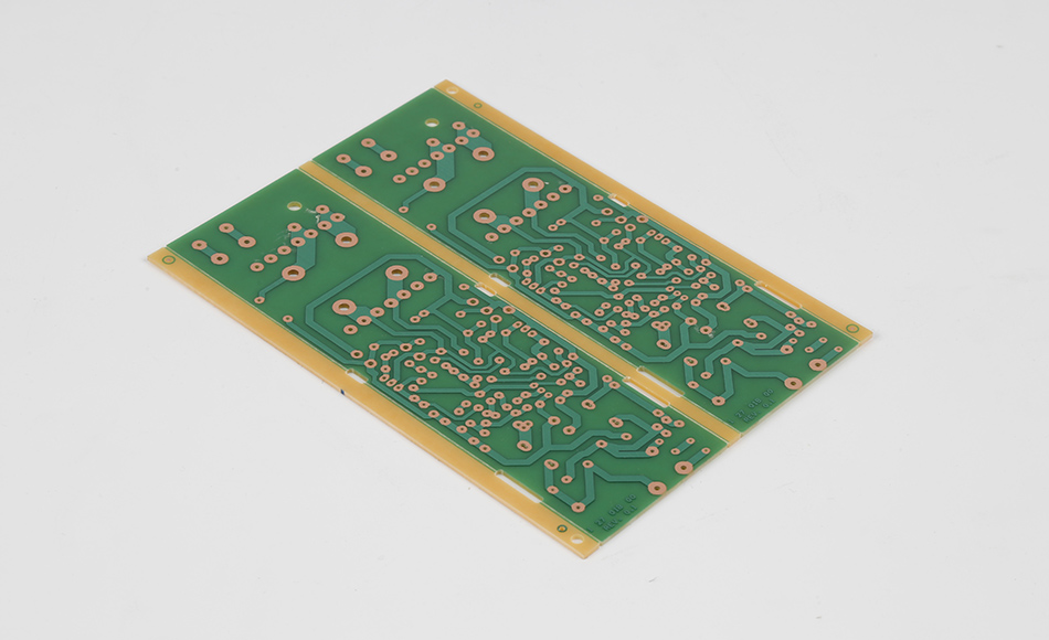
CEM3 PCB has evolved into a versatile substrate that excels beyond its traditional mid-tier applications, particularly in high-frequency electronics and harsh operational environments. As industries like telecommunications, automotive, and industrial automation demand faster data transmission and greater resilience, CEM3 PCB has undergone material and design innovations to meet these needs. Unlike FR4, which dominates high-end high-frequency applications but at a premium cost, CEM3 PCB offers a cost-effective solution with sufficient signal integrity for frequencies up to several gigahertz. Additionally, its inherent robustness, when optimized, allows it to withstand extreme temperatures, moisture, and mechanical stress—making it a reliable choice for outdoor and industrial settings. This article explores CEM3 PCB’s role in high-frequency signal transmission, its adaptations for harsh environments, integration with additive manufacturing, and emerging applications that leverage its unique balance of performance and affordability.
High-frequency electronics—including 5G routers, Wi-Fi 6E devices, and radar systems—require substrates that minimize signal loss and maintain consistent impedance. CEM3 PCB, once limited to low-frequency applications, now meets these demands through targeted material improvements:
The dielectric constant (Dk) and dissipation factor (Df) of a substrate directly impact signal integrity at high frequencies. CEM3 PCB’s epoxy resin is modified with low-loss additives, such as hollow glass microspheres or fluorinated polymers, to reduce Dk variation and lower Df. This ensures that signals propagate with minimal attenuation, even at frequencies up to 6 GHz. In 5G small cells, which operate in the 3.5 GHz and 28 GHz bands, this stability prevents data packet loss and maintains connection quality.
CEM3 PCB’s glass fiber structure is optimized to minimize unevenness in the substrate surface, which can cause signal reflection. The non-woven core, combined with tightly woven outer layers, creates a smoother surface for copper trace deposition, ensuring consistent impedance across the PCB. Additionally, advanced design techniques—such as controlled trace spacing and ground plane optimization—work with CEM3’s material properties to reduce crosstalk between adjacent traces. This is critical in high-density PCBs for IoT gateways, where multiple high-frequency signals travel in close proximity.
At high frequencies, electrical current tends to flow along the surface of copper traces (skin effect), increasing resistance and signal loss. CEM3 PCB addresses this by supporting thinner, higher-purity copper cladding (1/2 oz to 1 oz), which reduces conductor resistance while maintaining mechanical strength. The substrate’s thermal stability also prevents copper oxidation at high frequencies, ensuring consistent conductivity over time. In automotive radar systems (operating at 77 GHz), this combination of low conductor loss and thermal stability ensures accurate distance measurements.
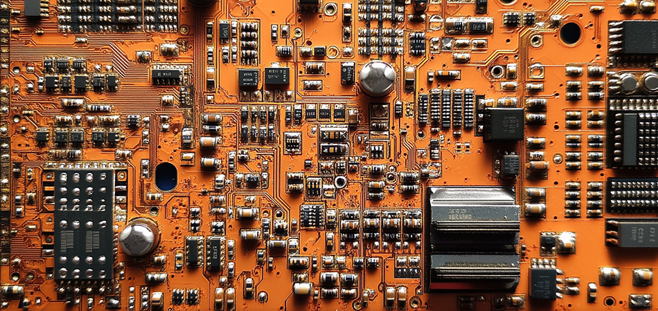
Many electronics operate in environments with extreme temperatures, moisture, vibration, or chemical exposure. CEM3 PCB is engineered to withstand these conditions, outperforming standard substrates in durability:
CEM3 PCB’s epoxy resin is formulated with heat-resistant additives, such as phenolic modifiers, to enhance its glass transition temperature (Tg). This allows it to maintain mechanical and electrical properties at temperatures up to 150°C, making it suitable for under-hood automotive electronics and industrial ovens. In electric vehicle (EV) battery management systems, which experience continuous heat generation, CEM3 PCB resists delamination and maintains stable performance.
Harsh environments often expose PCBs to humidity, water, or corrosive substances. CEM3 PCB’s resin is infused with hydrophobic agents, such as silane coupling agents, to repel moisture and prevent absorption. This reduces the risk of electrical shorts or dielectric breakdown in applications like marine sensors or agricultural monitors, which operate in damp conditions. Additionally, the glass fiber reinforcement resists chemical attack from oils, solvents, and fertilizers, extending PCB lifespan in industrial settings.
CEM3 PCB’s layered structure—non-woven core between woven glass layers—provides excellent flexural strength and impact resistance. This makes it resistant to vibration-induced fatigue, a common issue in aerospace and heavy machinery electronics. In drone navigation systems, which experience constant vibration during flight, CEM3 PCB prevents solder joint cracking and trace damage, ensuring reliable operation.
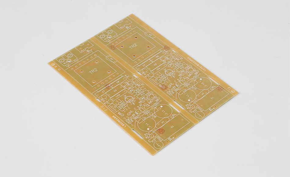
Advancements in manufacturing techniques have expanded CEM3 PCB’s capabilities, enabling higher precision and customization:
CEM3 PCB is compatible with additive manufacturing processes, such as inkjet printing of conductive inks and 3D printing of dielectric structures. This allows for rapid prototyping of complex high-frequency designs, where traditional subtractive manufacturing (etching) would be cost-prohibitive. For example, 3D-printed microvias in CEM3 PCBs enable vertical signal routing in high-density 5G modules, reducing size and improving performance. Additive manufacturing also supports on-demand production of low-volume, specialized CEM3 PCBs for industrial sensors, shortening development cycles.
Modern lamination for CEM3 PCB uses vacuum pressing and precise temperature control to eliminate air bubbles and ensure uniform resin distribution. This creates a denser substrate with improved mechanical and electrical properties. In multi-layer CEM3 PCBs—used in industrial controllers—this lamination process ensures strong interlayer bonding, preventing delamination under thermal or mechanical stress.
CEM3 PCB undergoes specialized surface treatments to enhance solderability and corrosion resistance. Immersion tin or electroless nickel immersion gold (ENIG) finishes protect copper traces from oxidation, ensuring reliable solder joints in high-moisture environments. For PCBs in outdoor lighting systems, these treatments extend maintenance intervals and reduce failure rates.
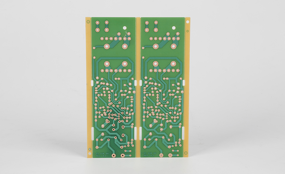
CEM3 PCB’s combination of high-frequency performance, durability, and affordability makes it ideal for diverse applications:
5G Small Cells: CEM3 PCB’s low signal loss and cost-effectiveness make it a staple in 5G small cells, which require widespread deployment to cover urban areas. Its ability to handle 3.5 GHz frequencies ensures seamless connectivity in dense environments.
Satellite Communication Terminals: These devices operate in outdoor, temperature-fluctuating conditions. CEM3 PCB’s thermal resistance and signal stability ensure reliable data transmission between ground stations and satellites.
PLCs and Motor Drives: Programmable logic controllers (PLCs) and motor drives in factories require durable PCBs that resist vibration and heat. CEM3 PCB’s mechanical strength and thermal stability prevent downtime in manufacturing lines.
Environmental Sensors: Sensors monitoring air quality, pressure, or chemical levels in industrial facilities use CEM3 PCB for its moisture resistance and reliability, ensuring accurate data collection in harsh conditions.
Smart Home Hubs: These devices integrate multiple high-frequency wireless modules (Wi-Fi, Bluetooth, Zigbee). CEM3 PCB’s signal integrity prevents interference, ensuring smooth communication between connected devices.
Outdoor Security Cameras: Exposed to rain, dust, and temperature swings, these cameras rely on CEM3 PCB’s durability to maintain 24/7 operation and high-quality video streaming.
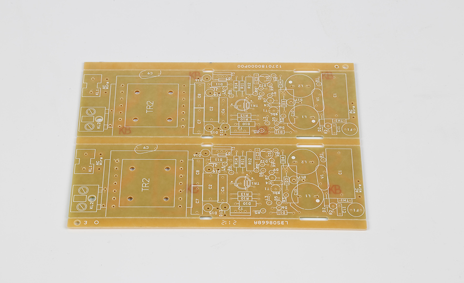
CEM3 PCB’s advantages become clear when compared to other substrates in key applications:
FR4 offers superior high-frequency performance but at 30–50% higher cost. For mid-range devices like home Wi-Fi routers (operating up to 6 GHz), CEM3 PCB provides sufficient signal integrity at a lower price, making it more accessible for mass production.
PTFE (Teflon) substrates excel at frequencies above 10 GHz but are expensive and difficult to process. CEM3 PCB is a practical alternative for applications up to 6 GHz, such as 5G routers, where PTFE’s performance is unnecessary.
vs. Metal-Core PCBs (MCPCBs) in High-Power Devices
MCPCBs dissipate heat better in high-power applications but are heavier and more costly. CEM3 PCB is preferable for low-to-moderate power devices like LED drivers (10–50W), offering sufficient thermal performance at a fraction of the cost.
FPCs are ideal for highly flexible designs but lack the mechanical strength of CEM3 PCB. For semi-rigid wearables like fitness trackers, CEM3 PCB provides enough flexibility for comfort while withstanding daily use.
Ongoing research and development are expanding CEM3 PCB’s capabilities, ensuring it remains relevant in emerging technologies:
Adding carbon nanotubes (CNTs) or graphene to CEM3’s epoxy resin could further reduce Df and improve thermal conductivity, extending its high-frequency performance to 10+ GHz. These nanocomposites also enhance mechanical strength, making CEM3 PCB suitable for even harsher environments.
Manufacturers are exploring bio-based epoxy resins—derived from plant oils or recycled plastics—and recycled glass fibers for CEM3 PCB. These sustainable variants maintain performance while reducing environmental impact, aligning with global initiatives to reduce electronics’ carbon footprint.
CEM3 PCB’s porous structure makes it compatible with energy-harvesting materials, such as piezoelectric films or thermoelectric generators. This could enable self-powered sensors, where the PCB both supports electronics and captures ambient energy (vibration, heat), reducing reliance on batteries.
CEM3 PCB has transcended its traditional role, emerging as a high-performance substrate for high-frequency electronics and harsh environments. Its ability to maintain signal integrity at gigahertz frequencies, combined with durability in extreme conditions, makes it a versatile choice for industries ranging from telecommunications to industrial automation. By balancing performance, cost, and manufacturability, CEM3 PCB enables innovations that would be impractical with more expensive substrates. As technology advances—demanding faster data transmission and greater resilience—CEM3 PCB will continue to evolve, solidifying its position as a critical material in the electronics ecosystem. For engineers and manufacturers, it represents a strategic solution that meets today’s challenges while enabling tomorrow’s breakthroughs.

Got project ready to assembly? Contact us: info@apollopcb.com


We're not around but we still want to hear from you! Leave us a note:

Leave Message to APOLLOPCB
