-
- PCB TYPE
- PRINTED CIRCUIT BOARD PROTOTYPE ALUMINUM PRINTED CIRCUIT BOARD R&F PCB FPC HIGH FREQUENCY PCB HIGH-TG PCB HEAVY COPPER PCB HDI PCB PCB FOR LIGHTING METAL CORE PCB
time:Aug 28. 2025, 19:19:09
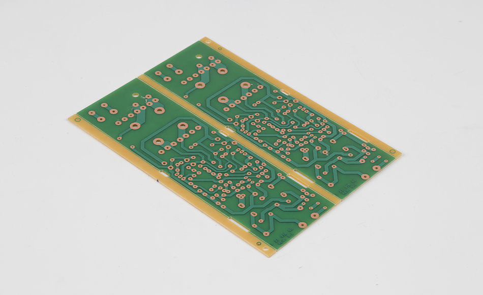
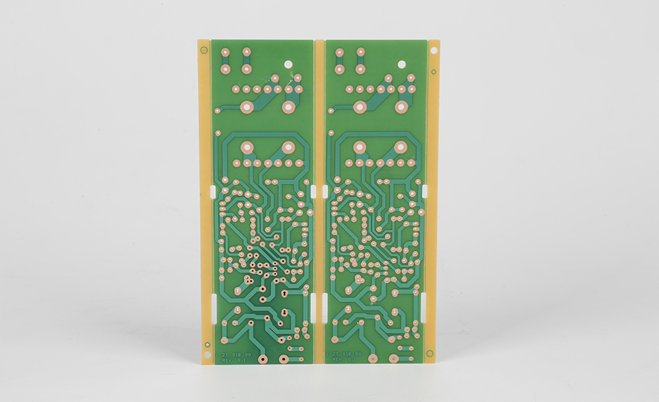
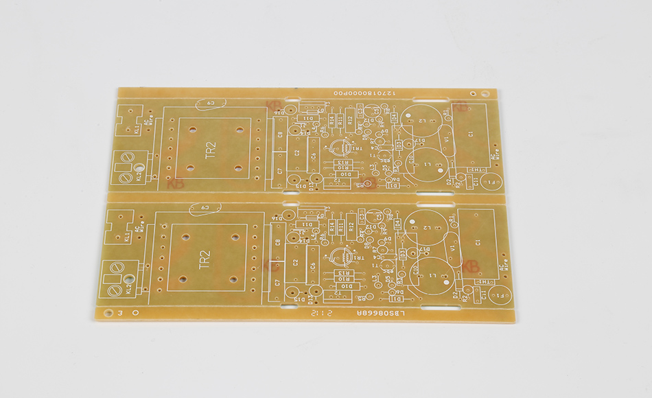
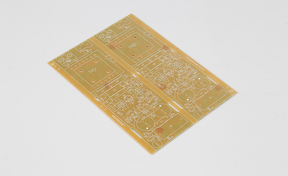
CEM3 PCB is a key substrate for high-mixed-signal systems—devices integrating analog, digital, and RF circuits. Unlike specialized substrates (high-frequency FR4, ceramic) that prioritize one signal type, it balances electrical performance, mechanical stability, and cost-effectiveness, suiting mid-tier applications like industrial test equipment, medical monitors, and smart grid controllers.
Signal integrity is critical for these systems: analog circuits are sensitive to digital noise, and RF modules need stable impedance. Generic PCBs lack dielectric stability or are too costly, while CEM3 PCB fills this gap with controlled dielectric properties, low signal loss, and mixed-component compatibility—affordable for mid-volume production.
This article explores how CEM3 PCB enables signal integrity (mitigating cross-talk, optimizing RF impedance), addresses design challenges, shares optimization strategies, and aligns with miniaturization trends—supporting engineers building robust mixed-signal electronics.
High-mixed-signal systems demand a substrate that handles three conflicting needs: isolate analog signals from digital noise, maintain RF impedance stability, and support dense components—all cost-effectively. CEM3 PCB meets these via three key attributes generic or specialized substrates lack.
Analog circuits (e.g., 12-bit precision temperature sensors) are vulnerable to EMI from high-speed digital components (e.g., 100 MHz microcontrollers). CEM3 PCB minimizes this:
Low Dielectric Loss (Df): Across DC (analog) to 2.4 GHz (RF), Df stays low (<0.02 at 1 MHz, <0.018 at 2.4 GHz), reducing signal attenuation for both signal types.
Stable Dielectric Constant (Dk): Dk variation is tight (±5%) vs. generic CEM1’s ±10%. A 2% Dk shift alters RF impedance by 4%, causing reflections—CEM3’s stability avoids this.
EMI Shielding Compatibility: Its glass-fiber/epoxy matrix supports EMI shielding (copper tape, conductive paint) between signal sections. Unlike flexible PCBs (FPCs), it retains structural integrity for consistent isolation.
Mixed-signal systems integrate diverse components: large analog capacitors, fine-pitch digital ICs, RF modules. CEM3 PCB’s mechanical traits support this:
Dimensional Stability: Low CTE minimizes reflow warpage. A 1.6mm CEM3 PCB keeps ±0.1mm accuracy post-reflow—critical for 0.5mm-pitch ICs and analog connectors.
Flat Surface: Smooth finish (Ra < 1.0μm) enables reliable soldering of through-hole (potentiometers) and surface-mount (RF modules) components, avoiding cold joints.
Load-Bearing Capacity: Supports heavy parts (50g RF shields) without flexing. Essential for vertically mounted industrial PCBs—flexing in generic PCBs breaks trace connections.
Specialized substrates (RF-optimized FR4, ceramic) cost 2–3x more than CEM3 PCB. For mid-volume (10,000–100,000 units/year) applications like medical monitors, CEM3 resolves cost issues:
Low Per-Unit Costs: 30–40% cheaper than RF-optimized FR4, delivering 80–90% signal performance. A 50,000-unit patient monitor line saves \(150k–\)200k annually.
High Yields: Compatible with standard manufacturing (wet etching, AOI) for 95%+ yields—higher than ceramic’s 85%. Reduces scrap and speeds time-to-market.
Simplified Design: Handles all three signal types, eliminating multi-substrate setups (analog/digital PCBs connected by cables). Cuts assembly complexity, EMI, and system cost by 15–20%.

While CEM3 PCB suits mixed-signal designs, conflicting signal types create unique challenges. Below are common issues and their impacts.
Cross-talk (unwanted signal coupling) degrades analog signals. High-frequency digital traces (100 MHz microcontroller buses) induce noise in 1mV analog sensor traces:
Reduced Precision: 50mV cross-talk corrupts 12-bit ADC inputs (0.24mV resolution), making sensor data unreliable.
False Triggers: Analog noise couples into digital clock traces, causing microprocessor errors (e.g., incorrect smart grid energy readings).
Dense layouts exacerbate this—designers place traces close to save space, increasing capacitance and coupling.
RF modules (Bluetooth Low Energy, Zigbee) need 50Ω (or 75Ω) impedance for maximum power transfer. CEM3’s stable dielectric properties still see mismatch from:
Trace Width Errors: 0.1mm deviation from calculated width (based on Dk) shifts impedance by 5–10%. For 2.4 GHz, this causes 10–20% reflection, cutting wireless range by 30–40%.
Layer Dk Variations: ±2% Dk differences between layers (e.g., RF trace on layer 1, ground on layer 2) create impedance steps, attenuating signals.
Component Parasitics: RF parts (antennas, transceivers) have pad capacitance/inductance. Unaccounted for, these add to trace impedance, degrading quality.
Ground bounce (voltage fluctuations) occurs when digital components switch, drawing transient currents. In CEM3 PCBs, shared ground planes spread this bounce to analog sections:
Analog Offset Errors: 100mV bounce shifts op-amp offsets. A medical temperature sensor could see 0.5°C inaccuracy—outside ±0.1°C limits.
RF Noise: Bounce injects noise into ground planes, coupling to RF traces. A 50mV bounce in Bluetooth modules raises BER from 10⁻⁶ to 10⁻⁴, causing retransmissions.

Designers can leverage CEM3’s strengths to resolve these challenges. Below are targeted strategies for each signal type.
Physical Separation: Keep analog/digital traces 3x the trace width apart (0.6mm for 0.2mm traces). CEM3’s stable dielectric cuts cross-talk by 40–50% vs. CEM1.
Guard Traces: Add 0.1mm grounded traces between sections, connected to analog ground every 5mm. Absorbs digital EMI before it reaches analog paths.
Layer Partitioning: In multi-layer PCBs, place analog traces on one layer, digital on another, with a ground plane in between (e.g., 4-layer: analog/layer1, ground/layer2, digital/layer3, power/layer4). Eliminates cross-talk for most designs.
Example: An industrial test equipment designer used 0.6mm separation and guard traces between a 12-bit ADC (analog) and 100 MHz bus (digital). Cross-talk dropped from 50mV to <5mV, restoring ADC precision to 0.1% of full scale.
Precise Trace Calculation: Use CEM3’s Dk (4.5–5.0) with impedance calculators (e.g., Polar Si9000). A 50Ω trace on 1.6mm CEM3 (1oz copper) needs ~0.8mm width—±0.05mm keeps impedance ±2%.
Controlled Routing: Avoid sharp bends (use 45° or curves) and stubs (<λ/20; λ=25mm for 2.4 GHz, so stubs <1.25mm). Prevents impedance discontinuities.
Parasitic Compensation: Use stub tuning for RF component pads. A Bluetooth module with 0.5pF parasitic capacitance needs a 0.1mm×0.8mm stub—adds inductance to restore 50Ω.
Case Study: A smart home sensor maker optimized 2.4 GHz traces (0.8mm width, curved routing). Wireless range rose from 20m to 35m, BER dropped from 10⁻⁴ to 10⁻⁶—meeting reliability targets.
Split Ground Planes: Divide ground into analog/digital sections, connected at a single "star" point (e.g., power supply input). Isolates analog ground from digital transients.
Low-Impedance Paths: Use wide, short ground traces for digital components. A 2mm trace (vs. 0.2mm) for 100 MHz microcontrollers cuts ground impedance by 80%, reducing bounce from 100mV to 20mV.
Decoupling Capacitors: Place 0.1μF X7R capacitors within 1mm of digital power pins, connected to digital ground. Supplies transient currents locally, reducing shared ground current.
Result: A medical device designer split the ground plane and added decoupling to a patient monitor PCB. Bounce dropped from 80mV to 15mV, eliminating op-amp errors and meeting ±0.1°C temperature accuracy.

CEM3 PCB’s signal integrity capabilities excel in three high-impact mixed-signal use cases.
Devices like data loggers integrate 8–16 analog sensors, 32-bit microcontrollers, and Wi-Fi modules. CEM3 PCB supports this by:
Analog Isolation: Split ground/guard traces protect 16-bit ADC data, achieving ±0.05% accuracy—on par with costly RF-optimized FR4.
Dense Layouts: 16 analog connectors, microcontroller, and Wi-Fi fit on 100mm×150mm CEM3—50% smaller than multi-substrate designs.
Harsh Environment Resistance: Dust/vibration resistance ensures 99.5% uptime vs. 95% for FPC-based equipment.
Case Study: An industrial firm replaced FR4 with CEM3 in 16-channel loggers. PCB cost fell 35%, size 40%, fitting tight factory enclosures while retaining accuracy.
Monitors combine analog ECG/SpO₂ sensors, DSPs, and Bluetooth modules. CEM3 PCB is critical for:
Patient Safety: Split ground planes isolate 0.5mV ECG signals from digital noise, ensuring accurate heart rate monitoring for arrhythmia detection.
Biocompatibility: Coatable with polyurethane (meets ISO 10993)—unlike porous ceramic substrates.
Cost-Effective Deployment: Low cost lets hospitals double monitor numbers, improving patient coverage.
Result: A medical maker used CEM3 for portable monitors. FDA clearance was granted (±1 bpm ECG accuracy), cost dropped 25%, making it accessible to rural clinics.
Controllers integrate analog current/voltage sensors, digital meter ICs, and LoRa modules. CEM3 PCB addresses key needs:
Accurate Measurement: Split ground planes isolate analog sensors from digital noise, keeping energy readings ±0.5% (meets utility standards).
Long-Range RF: Optimized LoRa trace impedance ensures 5–10km range—critical for rural grids.
Outdoor Durability: Low moisture absorption and UV stability enable 10+ year lifespans in utility boxes.
Case Study: A utility deployed 10,000 CEM3-based controllers. After 3 years, failure rates were 1.2% (vs. 8% for generic CEM1), saving $200k in replacements.

As mixed-signal electronics grow smaller and more complex, CEM3 PCB is adapting to new demands.
Thin-Core Variants: 0.4–0.6mm CEM3 retains 90% mechanical strength, suiting wearables (e.g., health monitors) and mini IoT sensors.
Fine-Pitch Support: Improved surface smoothness (Ra < 0.8μm) enables 0.3mm-pitch ICs—critical for AI edge devices with dense microchips.
mmWave Optimization: New CEM3 formulations reduce Df at 28–39 GHz (mmWave), expanding use to 5G small cells and radar modules.
Advanced Shielding: Integratable with thin-film metal shields (e.g., nickel-gold) for better RF isolation in high-frequency designs.
Recycled Materials: 25% recycled glass fibers (from wind turbine blades) reduce carbon footprint by 20%—without performance loss.
Bio-Based Resins: Plant-derived epoxies (castor oil) are being tested—retain Dk/Df stability and add biodegradability at end-of-life.

CEM3 PCB has established itself as a foundational substrate for high-mixed-signal electronics, solving the core challenge of balancing signal integrity, mechanical stability, and cost. Its controlled dielectric properties isolate analog, digital, and RF signals; mechanical traits support dense layouts; and affordability enables mid-volume production—filling a gap no generic or specialized substrate can match.
The optimization strategies outlined—cross-talk reduction via guard traces, RF impedance tuning, ground bounce mitigation—unlock CEM3’s full potential, ensuring designs meet strict reliability standards. Real-world applications prove its value: industrial equipment with 99.5% uptime, medical monitors with FDA clearance, smart grid controllers with 10+ year lifespans.
As mixed-signal systems evolve—toward miniaturization, higher frequencies, and sustainability—CEM3 PCB adapts. Thin-core variants, mmWave optimization, and eco-friendly formulations will keep it relevant for future applications, from 5G edge devices to smart city sensors.
For engineers, CEM3 PCB is more than a substrate—it is a strategic tool to build robust, cost-effective mixed-signal systems. In a market where signal integrity and affordability are non-negotiable, CEM3 PCB remains the go-to choice for mid-tier electronics, powering critical industries now and in the future.

Got project ready to assembly? Contact us: info@apollopcb.com


We're not around but we still want to hear from you! Leave us a note:

Leave Message to APOLLOPCB
