-
- PCB TYPE
- PRINTED CIRCUIT BOARD PROTOTYPE ALUMINUM PRINTED CIRCUIT BOARD R&F PCB FPC HIGH FREQUENCY PCB HIGH-TG PCB HEAVY COPPER PCB HDI PCB PCB FOR LIGHTING METAL CORE PCB
time:Jul 08. 2025, 10:25:20
In the dynamic realm of printed circuit board (PCB) technology, double layer aluminum PCBs with Hot Air Solder Leveling (HASL) finish represent a fusion of thermal efficiency, mechanical durability, and cost - effective manufacturing. This combination is particularly advantageous for applications that demand reliable heat management, robust electrical connectivity, and compatibility with high - volume production processes. This article explores the technical nuances of double layer aluminum PCBs with HASL finish, covering their structural design, material selection, manufacturing processes, quality assurance, and diverse applications, while highlighting their role in modern electronic systems.
Fundamentals of Double Layer Aluminum PCBs with HASL Finish
Structural Architecture
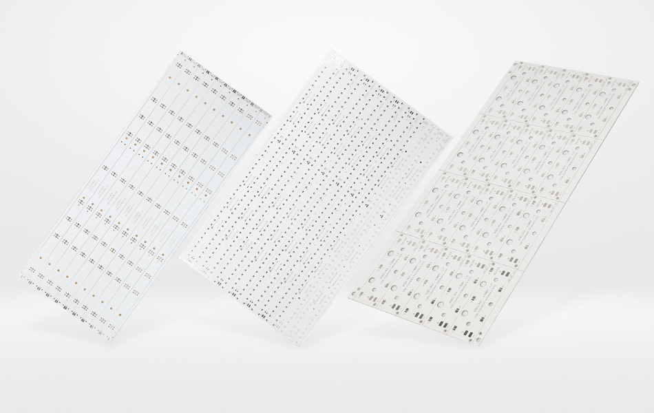
A double layer aluminum PCB consists of two copper conductive layers—top and bottom—separated by a dielectric layer bonded to an aluminum substrate. The aluminum base provides excellent thermal conductivity and mechanical support, while the two copper layers handle signal transmission and power distribution. The HASL finish adds a protective solderable coating to the copper traces, ensuring long - term reliability and ease of component soldering.
Aluminum Substrate Properties
Thermal Conductivity: Aluminum alloys, commonly from the 6xxx series, efficiently dissipate heat generated by high - power components, preventing thermal stress and ensuring stable component operation.
Mechanical Robustness: The aluminum substrate offers resistance to bending, vibrations, and impacts, making it suitable for harsh operating environments.
Formability: Allows for custom shapes and sizes, facilitating integration into diverse electronic enclosures.
HASL Finish Characteristics
Solderability: Creates a uniform layer of solder on copper traces, enabling reliable soldering of through - hole and surface - mount components.
Cost - Effectiveness: A widely adopted finish for high - volume production due to its balance of performance and affordability.
Corrosion Resistance: Protects copper from oxidation, ensuring long - term electrical integrity in humid or corrosive environments.
Key Advantages for Industrial Applications
Thermal - Electrical Balance: The double layer design combines aluminum's thermal benefits with HASL's soldering advantages, ideal for power - intensive circuits.
Manufacturing Efficiency: HASL's compatibility with wave soldering and reflow processes streamlines mass production, reducing assembly time and costs.
Reliability: Suitable for applications requiring consistent performance over extended periods, thanks to the aluminum substrate's durability and HASL's protective coating.
Material Selection and Layer Design
Aluminum Substrate and Dielectric Layer
Aluminum Alloy Selection
6xxx Series Alloys: Preferred for their balance of thermal conductivity (180 - 210 W/mK) and mechanical strength, enabling efficient heat dissipation and robust structural support.
Thickness Considerations: Thinner substrates (0.8 - 1.6mm) for compact designs; thicker substrates (2.0 - 3.0mm) for high - power applications requiring enhanced heat capacity.
Dielectric Layer Options
Ceramic - Filled Epoxies: Cost - effective with moderate thermal conductivity (1.5 - 2.5 W/mK), suitable for most industrial and consumer applications.
Polyimide Dielectrics: High - temperature resistant (up to 250°C), ideal for harsh environments but with higher cost, used in aerospace or automotive prototypes.
Copper Layers and HASL Finish
Copper Foil Properties
Thickness Optimization: 1 - 2 oz copper foil for signal traces; 3 - 4 oz for power paths to minimize voltage drops and heat generation.
Surface Preparation: Roughened copper surface before HASL application to enhance solder adhesion and coating uniformity.
HASL Process Chemistry
Flux Application: Activates copper surface to promote solder wetting, typically using rosin - based or water - soluble fluxes.
Solder Bath: Immersion in molten tin - lead or lead - free solder (e.g., Sn - Cu - Ni alloys) to form a thick, durable solder layer (5 - 15μm).
Hot Air Leveling: High - velocity air jets remove excess solder, creating a smooth, uniform finish with controlled thickness.
Design Considerations for Performance Optimization
Thermal Management Strategies
Component Placement
Top Layer: Mount high - power components (e.g., MOSFETs, LEDs) directly over the aluminum substrate to leverage direct heat transfer.
Bottom Layer: Reserve for heat sinks or thermal interface materials, using thermal vias to connect top - layer components to the aluminum base.
Via Design: Circular or square vias with diameters optimized for component power levels, spaced to avoid copper trace congestion.
Thermal Simulation
Finite Element Analysis (FEA): Models heat flow through the aluminum substrate and HASL - coated traces, identifying hotspots and optimizing via density.
Thermal Resistance Reduction: Use of thermal vias with copper plating to minimize thermal impedance between components and the aluminum base.
Electrical Design Principles
Trace Routing
Top Layer: High - speed signals with controlled impedance (50 - 100Ω), routed away from power traces to reduce crosstalk.
Bottom Layer: Solid ground plane to act as a return path for signals, reducing electromagnetic interference (EMI) and improving signal integrity.
Power Traces: Wide, straight routes on both layers for low - impedance power distribution, with isolation from signal traces.
Ground and Power Planes
Star Grounding: Centralized grounding point for analog and digital circuits to prevent ground loops, critical in precision measurement applications.
Decoupling Capacitors: Placed close to power pins on the top layer, with short traces to the bottom ground plane for effective noise filtering.
Mechanical and Environmental Design
Mounting and Form Factor
Mounting Holes: Reinforced with annular rings to prevent substrate cracking, positioned at stress - free zones (avoiding corners and component clusters).
Edge Clearance: Minimum 1mm from board edges for trace routing, ensuring mechanical stability and compatibility with enclosures.
Environmental Protection
Conformal Coating: Optional after HASL to protect against moisture and chemicals, with acrylic or silicone coatings compatible with the solder finish.
Thermal Cycling Resistance: Aluminum's low coefficient of thermal expansion (CTE ~23ppm/°C) reduces stress on solder joints during temperature fluctuations.
Manufacturing Processes for Double Layer Aluminum PCBs with HASL Finish
Pre - Production Design
CAD Tools and Gerber Preparation
Layout Software: Altium Designer, OrCAD, or KiCad for 2D/3D modeling, with thermal via placement and HASL - specific pad design (round or oval pads for better solder flow).
Gerber File Validation: Check for trace width consistency, via alignment, and HASL mask accuracy to avoid coating over non - solderable areas.
Material Preparation and Lamination
Aluminum Substrate Processing
Cutting: CNC milling or waterjet cutting for precise dimensions, followed by surface cleaning with alkaline solutions to remove oils and oxides.
Dielectric Lamination: High - pressure lamination (100 - 150°C, 50 - 100 psi) to bond ceramic - filled epoxy or polyimide sheets to the aluminum base, ensuring void - free adhesion.
Copper Layer Fabrication
Foil Lamination and Photolithography
Copper Foil Bonding: Electrolytic copper foil (18 - 70μm) laminated to both dielectric surfaces using thermal - cured adhesives.
Photoresist Application: Liquid or dry film photoresist applied to copper layers, exposed via UV light through a mask, and developed to define trace patterns.
Etching and Stripping
Chemical Etching: Ferric chloride or ammonium persulfate solutions to remove unprotected copper, leaving the designed traces with 10 - 15% overetch allowance for precision.
Resist Stripping: Alkaline solutions to remove remaining photoresist, followed by deionized water rinsing to prepare for HASL.
HASL Finish Application
Pre - Treatment
Desmear and Microetch: Removes drilling residues and roughens copper surface for better solder adhesion, using potassium permanganate or sulfuric acid solutions.
Flux Coating: Dipping or spraying of activated flux to prevent re - oxidation and promote solder wetting.
Solder Leveling
Solder Bath Temperature: 230 - 260°C for lead - free solder, 220 - 240°C for tin - lead, with immersion time of 3 - 5 seconds.
Hot Air Nozzles: Adjustable air pressure (0.5 - 1.5 bar) to form uniform solder layers, with special attention to via openings and pad edges.
Post - Processing
Cleaning and Inspection
Flux Residue Removal: Water - based cleaning to remove flux residues, critical for preventing long - term corrosion under the HASL coating.
AOI Inspection: Automated optical inspection for trace defects, solder bridging, or coating inconsistencies, using machine vision to verify HASL uniformity.
Quality Assurance and Testing
Electrical Performance Testing
Continuity and Impedance
Bed - of - Nails Testing: Verifies electrical connectivity between layers and traces, with a focus on via resistance (<50mΩ for reliable thermal pathways).
Impedance Testing: Network analyzers to measure characteristic impedance of high - speed traces, ensuring compliance with design specifications (±10% tolerance).
High - Voltage Testing
Dielectric Withstand Voltage: 500 - 1000V DC applied between copper layers and the aluminum substrate to check for insulation integrity, with leakage current <1μA.
Thermal Performance Validation
Infrared Thermography
Temperature Mapping: Identifies hotspots during full - load testing, ensuring component temperatures remain below maximum ratings (e.g., <125°C for most semiconductors).
Thermal Resistance Measurement: Hot Disk or transient thermal tests to quantify thermal impedance from components to the aluminum substrate (<5°C/W for efficient dissipation).
Thermal Cycling
Temperature Range: -40°C to +85°C for 100 - 500 cycles, checking for solder joint cracks or dielectric delamination using X - ray microscopy.
Mechanical and Environmental Testing
Bend and Vibration Tests
Bend Radius Testing: Minimum bend radius of 5 - 10x substrate thickness to ensure no trace cracking, critical for portable device prototypes.
Vibration Testing: Sinusoidal or random vibration (10 - 2000Hz, 2G acceleration) to assess mounting hole integrity and component retention.
Salt Spray and Humidity Tests
Salt Spray (ASTM B117): 5% NaCl solution for 24 - 1000 hours, evaluating HASL coating corrosion resistance (no copper oxidation or solder pitting).
Humidity Testing (85% RH, 85°C): Measures insulation resistance degradation over time, ensuring HASL - coated traces maintain >10MΩ impedance.
Applications of Double Layer Aluminum PCBs with HASL Finish
Industrial Power Electronics
Motor Drives and Inverters
HASL Advantages: Facilitates wave soldering of large through - hole capacitors and inductors, while the aluminum substrate dissipates heat from IGBTs and diodes.
Design Focus: Wide power traces on both layers, with thermal vias under switching devices to prevent thermal runaway.
Industrial Controllers
Reliability Needs: HASL's corrosion resistance suits dusty, humid factory environments, while the double layer design ensures stable signal transmission for PLCs and sensors.
Consumer Electronics
High - Power LED Lighting
HASL Benefits: Enables cost - effective mass production of LED panels, with HASL - coated traces ensuring reliable solder joints for high - brightness LED arrays.
Thermal Design: Top - layer LED placement with bottom - layer heat sinks, connected via thermal vias to maintain <80°C junction temperatures.
Audio Amplifiers
Signal Integrity: Bottom - layer ground plane reduces noise in audio traces, while HASL's smooth surface allows precise soldering of fine - pitch op - amps and capacitors.
Automotive Electronics
Engine Control Units (ECUs)
Environmental Resistance: HASL's durability and aluminum's vibration resistance meet automotive standards (e.g., AEC - Q100), with thermal vias managing heat from microprocessors.
Manufacturing Compatibility: High - volume wave soldering for through - hole connectors, critical for ECU reliability in engine bays.
Automotive Lighting
Thermal Management: Double layer design with HASL - coated traces for taillights and headlights, ensuring long - term performance in temperature extremes (-40°C to +125°C).
Renewable Energy Systems
Solar Inverters
Power Handling: Thick copper traces with HASL finish for low - resistance power paths, combined with aluminum substrate for heat dissipation from MOSFETs and diodes.
HASL Durability: Resists corrosion from moisture in outdoor installations, maintaining electrical integrity over 20+ years of operation.
Wind Turbine Controls
Vibration Resistance: Aluminum substrate and HASL - coated boards withstand mechanical stresses in turbine nacelles, with thermal vias ensuring stable operation of control electronics.
Market Trends and Technological Advancements
Shift to Lead - Free HASL
Regulatory Compliance: RoHS and REACH directives driving adoption of lead - free solder alloys (e.g., Sn - 3.0Ag - 0.5Cu), requiring adjustments in HASL process temperatures and flux formulations.
Performance Improvements: Lead - free HASL now matches tin - lead in solderability and thermal cycling resistance, thanks to nano - composite fluxes.
Integration with Advanced Manufacturing
Automated HASL Lines: Robotic flux application and solder bath control for consistent coating thickness, reducing human error in high - volume production.
Laser - Assisted HASL: Precise flux deposition on micro - vias and fine - pitch pads, enabling miniaturization in IoT and wearable devices.
Thermal Management Innovations
Hybrid Substrates: Aluminum combined with graphite or carbon fiber for enhanced thermal conductivity (300 - 400 W/mK), suitable for next - generation power modules.
Micro - Channel Cooling: Embedded fluid channels in aluminum substrates, integrated during lamination, for high - density power applications.
Environmental Sustainability
Recyclable Materials: Development of bio - based dielectrics and recycled aluminum substrates, with HASL processes using water - based fluxes to reduce chemical waste.
Energy - Efficient HASL: Low - temperature solder baths and waste heat recovery systems, aligning with global carbon reduction goals.
Conclusion
Double layer aluminum PCBs with HASL finish represent a pragmatic solution for applications demanding a blend of thermal efficiency, electrical reliability, and cost - effective manufacturing. The combination of aluminum's superior heat dissipation and HASL's robust solderability makes them ideal for diverse industries, from industrial power electronics to consumer devices. As technology evolves toward higher power densities and stricter environmental standards, advancements in material science and manufacturing processes will further enhance their performance, ensuring they remain a mainstay in modern PCB design. By leveraging their structural simplicity and functional versatility, engineers can create reliable, high - performance electronic systems that meet the challenges of today's and tomorrow's technological landscape.

Got project ready to assembly? Contact us: info@apollopcb.com


We're not around but we still want to hear from you! Leave us a note:

Leave Message to APOLLOPCB
