-
- PCB TYPE
- PRINTED CIRCUIT BOARD PROTOTYPE ALUMINUM PRINTED CIRCUIT BOARD R&F PCB FPC HIGH FREQUENCY PCB HIGH-TG PCB HEAVY COPPER PCB HDI PCB PCB FOR LIGHTING METAL CORE PCB
time:Jun 21. 2025, 09:20:04
In the ever - advancing electronics industry, the pursuit of smaller, more powerful, and energy - efficient devices has led to the development of innovative Printed Circuit Board (PCB) technologies. High Density Multi - Layer Al PCBs represent a significant leap forward, combining the high - performance attributes of multiple copper layers with the superior thermal management capabilities of an aluminum base. These PCBs are engineered to meet the complex electrical and thermal demands of modern electronics, enabling the creation of compact, yet highly functional devices. This article will comprehensively explore High Density Multi - Layer Al PCBs, delving into their structure, design principles, manufacturing processes, diverse applications, market dynamics, and future trends.
Understanding the Structure of High Density Multi - Layer Al PCBs
Layer Composition and Stack - up
A High Density Multi - Layer Al PCB features a complex stack - up of layers, typically consisting of multiple alternating copper and dielectric layers, with an aluminum core integrated within. The copper layers serve as the foundation for electrical circuitry, providing pathways for signal transmission and power distribution. These layers are patterned with intricate traces, pads, and planes, allowing for the connection of various electronic components.
Sandwiched between the copper layers are dielectric materials, which act as insulators, preventing electrical short - circuits while also facilitating the transfer of electromagnetic signals. The dielectric layers are carefully selected for their electrical properties, such as dielectric constant and dissipation factor, to ensure optimal signal integrity.
The aluminum core, strategically placed within the stack - up, serves as a robust heat sink. Its high thermal conductivity enables rapid heat dissipation from heat - generating components, preventing thermal bottlenecks that could degrade device performance. The aluminum core also provides mechanical strength and stability to the PCB, making it suitable for use in demanding environments.
Key Advantages
High Density Multi - Layer Al PCBs offer several distinct advantages over traditional PCBs. Firstly, the increased number of copper layers allows for a more compact circuit design. With multiple layers available, designers can route traces in a more organized manner, reducing the overall footprint of the PCB. This is particularly beneficial in applications where space is at a premium, such as in portable electronics and wearable devices.
Secondly, the integration of an aluminum core enhances thermal management. In high - density circuits, components are often packed closely together, leading to increased heat generation. The aluminum core efficiently absorbs and distributes this heat, maintaining lower operating temperatures and extending the lifespan of the components.
Moreover, the multi - layer structure enables better signal integrity. By separating power and ground planes, and routing high - speed signals on dedicated layers, electromagnetic interference (EMI) can be minimized. This results in more reliable signal transmission, which is crucial for applications involving high - speed data transfer, such as in telecommunications and data centers.
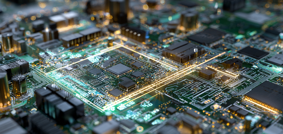
Design Principles for High Density Multi - Layer Al PCBs
Thermal Design
Component Placement and Heat - Transfer Paths
In the design of High Density Multi - Layer Al PCBs, component placement is a critical factor in thermal management. Heat - generating components should be positioned to maximize heat transfer to the aluminum core. This may involve placing them in close proximity to the core or using thermal vias to create direct pathways for heat flow. Additionally, components should be arranged in a way that promotes natural or forced - air cooling, ensuring that heat can be effectively dissipated from the PCB surface.
Thermal Via Design and Optimization
Thermal vias play a crucial role in facilitating heat transfer between the components and the aluminum core. These vias are small holes filled with highly conductive materials, such as copper, that connect different layers of the PCB. The design of thermal vias, including their size, number, and distribution, needs to be carefully optimized based on the heat - generating characteristics of the components and the overall thermal requirements of the design. By strategically placing thermal vias, designers can enhance the efficiency of heat transfer and prevent hotspots from forming on the PCB.
Electrical Design
Trace Routing and Impedance Control
Trace routing in High Density Multi - Layer Al PCBs requires meticulous planning to ensure signal integrity. With multiple layers available, designers have more flexibility in routing traces, but they also need to consider factors such as impedance control, crosstalk, and signal attenuation. For high - speed signals, impedance - controlled traces are essential to maintain consistent signal quality. Designers must carefully calculate the trace width, length, and spacing, as well as the dielectric constant of the insulating layers, to achieve the desired impedance values.
Power and Ground Plane Design
Power and ground plane design is a key aspect of electrical design for High Density Multi - Layer Al PCBs. The multi - layer structure allows for the creation of dedicated power and ground planes, which help to distribute electrical power evenly across the board and reduce electromagnetic interference. Well - designed power and ground planes can also improve the overall stability of the electrical supply, ensuring that components receive a consistent voltage. Designers need to ensure that the power and ground planes are continuous, with minimal splits or gaps, and that proper grounding techniques are employed to enhance the electrical performance of the PCB.
Design for Manufacturability
To ensure efficient production, High Density Multi - Layer Al PCB designs must adhere to the principles of design for manufacturability (DFM). Designers need to consider factors such as the minimum trace width and spacing that can be achieved during manufacturing, the maximum aspect ratio for vias, and the ease of component placement and soldering. By optimizing the design for manufacturability, potential production issues can be avoided, production costs can be reduced, and the time - to - market can be shortened. This may involve simplifying complex circuit layouts, using standard component footprints, and ensuring that the design is compatible with the manufacturing equipment and processes used by the PCB manufacturer.
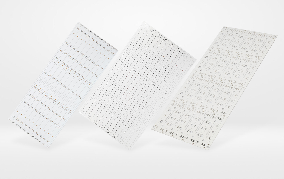
Manufacturing Processes of High Density Multi - Layer Al PCBs
Material Selection
The manufacturing process of High Density Multi - Layer Al PCBs begins with the careful selection of materials. High - quality copper foils are chosen for the electrical layers, ensuring excellent electrical conductivity and reliable signal transmission. The dielectric materials used between the copper layers are selected based on their electrical insulation properties, thermal stability, and ability to support high - density circuit designs.
For the aluminum core, high - purity aluminum sheets with consistent thickness and excellent thermal conductivity are preferred. Additionally, specialized adhesives and prepregs are used to bond the layers together, ensuring a strong and reliable structure.
Lamination
Lamination is a critical step in the manufacturing process, where the individual layers of the PCB are bonded together. Heat and pressure are applied to cure the adhesives and prepregs, creating a cohesive and stable structure. Precise control of lamination parameters, such as temperature, pressure, and time, is essential to ensure a uniform bond and avoid defects such as voids, delaminations, or uneven bonding. Any imperfections in the lamination process can significantly impact the electrical and thermal performance of the final PCB.
Drilling and Plating
After lamination, drilling is performed to create holes for vias, component mounting, and electrical connections. High - precision drilling machines are used to ensure accurate hole placement and clean hole walls. Following drilling, the holes are plated with copper to create electrical connections between the different layers of the PCB and to provide a solderable surface for component attachment. The plating process, typically electroplating, requires careful control of parameters such as current density, plating time, and temperature to achieve a uniform and reliable copper deposit.
Circuit Patterning
Circuit patterning is the process of creating the electrical circuits on the copper layers. Photolithography is commonly used for this purpose. A photosensitive resist material is applied to the copper surface, and then a patterned mask is used to expose the resist to ultraviolet (UV) light. The exposed areas of the resist are chemically altered and removed during the development process, leaving the unexposed resist in the shape of the circuit pattern. The remaining copper is then etched away using an etching solution, leaving only the copper traces and planes that form the electrical circuits.
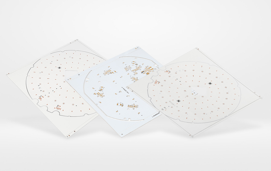
Applications of High Density Multi - Layer Al PCBs
Consumer Electronics
In the consumer electronics market, High Density Multi - Layer Al PCBs are widely used in devices such as smartphones, tablets, laptops, and smartwatches. These devices require compact, high - performance PCBs that can support a large number of components and handle complex electrical and thermal requirements. The high - density design of these PCBs allows for the integration of multiple functions into a small form factor, while the aluminum core ensures efficient heat dissipation, preventing performance throttling and extending the lifespan of the devices.
Telecommunications
The telecommunications industry relies on High Density Multi - Layer Al PCBs for base stations, routers, and other network equipment. These applications demand PCBs that can handle high - speed data transfer, complex signal processing, and efficient power management. The multi - layer structure of these PCBs enables better trace routing and impedance control for high - speed signals, while the aluminum core helps to dissipate the heat generated by high - power components, ensuring stable and reliable operation.
Aerospace and Defense
Aerospace and defense applications require PCBs that can perform reliably in extreme environments. High Density Multi - Layer Al PCBs are well - suited for these applications due to their high thermal conductivity, mechanical strength, and ability to support complex electrical circuits. They are used in aircraft avionics systems, satellite communication equipment, and military radar systems, where the ability to manage heat effectively, maintain signal integrity, and withstand mechanical stress is crucial for mission success.
Medical Electronics
In the medical electronics field, High Density Multi - Layer Al PCBs are used in a variety of devices, including diagnostic equipment, monitoring devices, and surgical instruments. These applications require PCBs that are compact, reliable, and capable of handling sensitive electrical signals. The high - density design of these PCBs allows for the integration of multiple sensors and components, while the aluminum core ensures efficient heat dissipation, which is essential for maintaining the accuracy and reliability of medical devices.
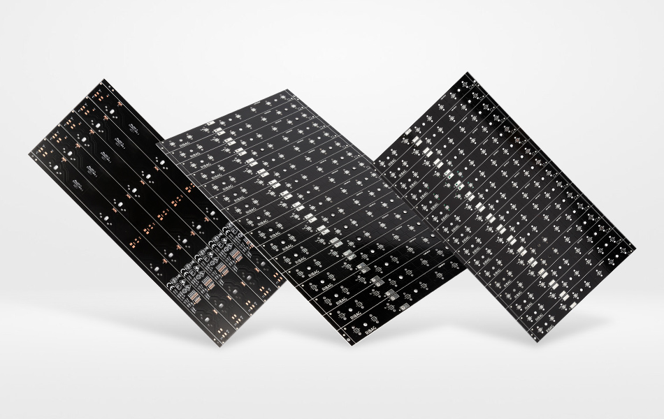
Market Dynamics of High Density Multi - Layer Al PCBs
Market Growth
The global market for High Density Multi - Layer Al PCBs has been experiencing significant growth in recent years, and this trend is expected to continue. The increasing demand for portable and high - performance electronics, the growth of the telecommunications industry, and the advancements in aerospace and defense technologies are all driving factors behind this growth. As more industries require PCBs that can meet the complex electrical and thermal demands of modern electronics, the market for High Density Multi - Layer Al PCBs is likely to expand further in the coming yCompetitive Landscape
The market for High Density Multi - Layer Al PCBs is highly competitive, with numerous manufacturers vying for market share. Key players in the market include both established PCB manufacturers with extensive experience and emerging companies that are bringing innovative technologies and manufacturing processes to the table. Competition is based on factors such as product quality, performance, cost - effectiveness, technological innovation, and customer service. Manufacturers are constantly investing in research and development to improve the performance of their PCBs, reduce production costs, and offer customized solutions to meet the specific requirements of different customers and industries.
Challenges and Future Trends
Challenges
Despite their many advantages, the High Density Multi - Layer Al PCB industry faces several challenges. One of the main challenges is the cost. The use of high - quality materials, complex manufacturing processes, and advanced design techniques can result in relatively high production costs. Additionally, as electronics continue to evolve towards smaller form factors and higher levels of integration, the design and manufacturing of High Density Multi - Layer Al PCBs become more complex, requiring more advanced design tools and skilled engineers.
Another challenge is ensuring consistent quality during mass production. The high - density nature of these PCBs makes it more difficult to detect and correct manufacturing defects, which can impact the performance and reliability of the final products.
Future Trends
The future of High Density Multi - Layer Al PCBs is filled with exciting possibilities. Advancements in materials science are expected to lead to the development of new copper alloys, dielectric materials, and aluminum composites with enhanced electrical, thermal, and mechanical properties. These new materials will further improve the performance of High Density Multi - Layer Al PCBs, enabling the creation of even more compact and powerful electronic devices.
The integration of emerging technologies, such as 5G, the Internet of Things (IoT), and artificial intelligence (AI), will create new opportunities for High Density Multi - Layer Al PCBs. These technologies will require PCBs that can support high - speed data transfer, complex signal processing, and intelligent thermal management, which are the key strengths of High Density Multi - Layer Al PCBs.
The adoption of advanced manufacturing technologies, such as additive manufacturing and automation, is also set to revolutionize the production of High Density Multi - Layer Al PCBs. Additive manufacturing could enable more complex and customized designs, while automation will improve production efficiency, reduce costs, and enhance quality control. Moreover, the growing focus on environmental sustainability will likely drive the development of more eco - friendly manufacturing processes and materials for High Density Multi - Layer Al PCBs, making them more attractive in the market.
Conclusion
High Density Multi - Layer Al PCBs have emerged as a game - changing technology in the electronics industry, offering a unique combination of high - density circuit design, excellent thermal management, and reliable electrical performance. Their applications span across a wide range of industries, from consumer electronics and telecommunications to aerospace, defense, and medical electronics. While facing challenges related to cost and manufacturing complexity, the future of High Density Multi - Layer Al PCBs is bright, with ongoing advancements in materials, manufacturing technologies, and emerging trends presenting numerous opportunities for growth and innovation. As the electronics industry continues to evolve, High Density Multi - Layer Al PCBs will undoubtedly play an increasingly important role in enabling the development of more advanced, compact, and efficient electronic systems.

Got project ready to assembly? Contact us: info@apollopcb.com


We're not around but we still want to hear from you! Leave us a note:

Leave Message to APOLLOPCB
