-
- PCB TYPE
- PRINTED CIRCUIT BOARD PROTOTYPE ALUMINUM PRINTED CIRCUIT BOARD R&F PCB FPC HIGH FREQUENCY PCB HIGH-TG PCB HEAVY COPPER PCB HDI PCB PCB FOR LIGHTING METAL CORE PCB
time:May 10. 2021, 18:46:03
Cost saving in every step of any engineering product development is very crucial by the first day. All steps of electronic product development including circuit design, PCB design, manufacturing, assembling and fixing into final product has no exception. The PCB developers demand always to keep manufacturing cost low and low. For this purpose every developer adopts all methods to save money at every step. The PCB manufacturers understand this psyche of product developers very well. This is why they guide their customers at every step to produce maximum number of PCBs and best usable techniques in a competitive price amount. This motivates and encourages the industry partners in product development. Every aspect of PCB manufacturing has variety of options and their pitfalls.
To reduce cost to some extent PCB development customers combine more than one PCB design files into one final file and then generate Gerber files. Gerber format is one of the most leading formats understood by the manufacturers. To produce one PCB Gerber file data after adding multiple PCB designs i.e., array of PCB designs is called PCB Panelization. PCBs are panelized after designing all PCBs and before to generating gerber data. It is usually done in two different ways:
1- Multiple copies of same PCB are combined in one PCB i.e., an array of PCBs.
In this case the extra charges are not added in manufacturing price. It is very popular in high production setups.
2- Different PCB designs are combined to one PCB file
APOLLOPCB Request PCB Panelization Service
In this method multiple different designs are added to same PCB panel. It becomes slightly complicated task for manufacturer to cut, package and ship different PCBs. An additional cost is added to total manufacturing cost of PCB. Customers generate one gerber file rather than multiple gerber files to save one time manufacturing cost. However, as a whole, it gives benefit to customer to save a handsome amount at manufacturing PCB phase. Both can be used for cost saving strategies for prototype testing and small scale PCB productions.
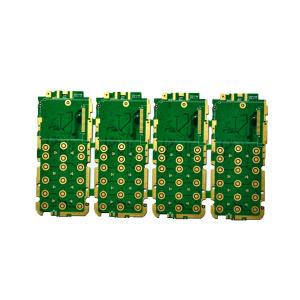
Figure 1: 4 to 1 PCB Panelization of same PCB-design
Figure 2: Panelization of two different PCB-designs
Generally, in good CAD software tools multiple PCBs can be panelized after discussion with manufacturer. Figure 1 and Figure 2 shows two different approaches for PCB Panelization.
PCB Panelization gives great benefits to PCB producers. It saves cost as well as assembly time, human effort, material cost and hence time-to-market of product.
A PCB for large scale production purposes i.e., for massive production of single PCB in form of PCB array is connected together physically as in Figure 1 and Figure 2. It makes it easier to move PCBs array across the assembly line much like a electronic component tray. The individual boards are easily separable after assembling for QC-inspection or to fit into the product enclosure. For production of tens of thousands of PCBs, component placement for PCB Panelization also does matter. Especially connectors and components hanging off the boundaries of PCB can create difficulty in PCB assembling process.
PCB Shape and size
Some PCB assembly contractors require minimum size of PCB to fit in a conveyor. A smaller size PCB which cannot fit physically within conveyor is needed to add small catch-in-hold area for processing. This extra PCB area is removed after PCB assembling. The situation is more complex in case of odd shaped PCBs. The rectangular PCB shape does fit easily in a panel however curved and odd-shaped PCBs need also some extra PCB area for handing by SMT conveyor. This situation can complicate PCB Panelization or assembly. Rectangular PCBs can be placed ideally both in vertical and horizontal axis. The CAD Software tools alongwith guidance of manufacturer and assembler can lead to early time measures. By involving manufacturer, assembly and PCB design engineer maximum benefits can be reaped.
APOLLOPCB Panel Space
APOLLOPCB run standard panels sizes like 24 x 18 inches. They need 0.5 inches clearance from components on the perimeter of panel. So 23 x 17 inches Panel size is actually available panel space for manufacturing. They need small gaps i.e., 0.1 inches for routing board arrays which is another unusable panel space. The PCB developer may get help to use panel space effectively by using calculation Tools available by manufacturers or online. PCB panel area is shown in Fig 4.
Figure 4: Standard (24 x18 inches) PCB panale area
A V-groove is way to split panelized PCBs. It is a small “V”-shaped cut on top and bottom side of panel leaving a small easily breakable base pcb raw material. The PCBs remain intact unless they are separated by applying a small force. The advantage of V-grooves is the distance between two boards is 0 inches.
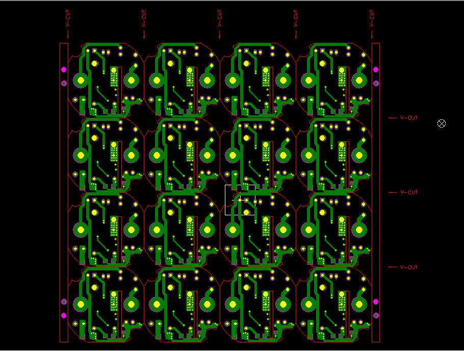
Figure 5: Breaking cut-in-hold part from PCB.
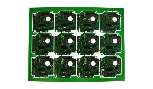
Figure 6: Removing cut-in-hold part from PCB
Figure 5 and Figure 6 show breaking and removing the cut-in-hold PCB area from actual usable PCB area.
1- The Panelization is much popular among producers for cost and time saving, ease of shipment, easy fitting into assembly plants etc.
2- It saves standard workable area for PCB manufacturing.
3- Prototype PCB panels can add multiple different designs. It saves one time cost which is applicable by manufacturer. So multiple PCBs can be made in one go only on extra cost.
4- In assembling process the Panelizationprotects PCBs from vibration and shock jerks.
5- Maximum PCBs can be manufactured form a standard size panel.
Request PCB Panelization Service
Panelization of printed circuit board has consideration with PCB manufacturing efficiency. Printed circuit boards are required to be kept safe during manufacturing, shipping and assembly process to avoid damaging of unit.Panelization contribute two factors to the manufacturing of board, one is the lead time of manufacturing can be reduced. Another advantage that panelization offers is, it is an aid for manufacturing of small printed circuit boards of irregular shapes. In broader sense the product quality can be controlled easily. The size of printed circuit board panel must confirm with the manufacturing ability of unit. It should have capabilities of automation equipment including paste printer, SPI system, re-flow oven, wave soldering machine. Some irregular printed circuit board of smaller sizes cannot be panelized.
A paramount problem which has been consistent in the process panelization of printed circuit board, the prototype pcb assembly fail to take consideration of manufacturing in terms of cost. This method has to depend on the combination methods according to the printed circuit boards requirements.
Some combination method of panelization
This method is the vastly used panelization method. It brings lots of advantages as far manufacturing of the printed circuit board is concern. First and foremost advantage is that, it is compatible in all situations, with no consideration to be taken of SMT manufacturer fabrication conditions and product combination. Another advantage is there is no influence of manufacturing item numbers on panelization. There is a unique process for some components of printing stencil design, because of panelization the printing quality will not diminish because of orientation of pad. For manufacturing of printed circuit board the cost of panelization is acceptable by manufacturers and the highest quality level of boards can be maintained.
Rotation Angle Panelization:
This is basically a material saving method from waste. In order to make the material utilization optimum, panelization is implemented by rotating 90 or 180 degrees. This method is called rotation angle panelization. The method of rotation angle panelization also offers some disadvantages. The mounting efficiency in printed circuit board manufacturing is decreased by method of rotation angle panelization and mounting quality will not a part of consideration in stable state. If the state is stable the visual inspection method of quality check is providing good results and on the other hand because of continuous rotation for the operator it is difficult to have observation regarding printed circuit board and chances of error in inspection result would increase. Ultimately it decreases the quality of board.
In this method of panelization both sides of the printed circuit board are panelization on one side as a panel. This method panelization is used in case where the volume of board on either size is not large and the heat resistivity of component is very poor. It has some advantages. It increases the efficiency of the process and also decreases manufacturing cost. Double layer printed circuit board in one-time craft, it cause saving of printing stencil and increases the utilization efficiency of the SMT equipments. The manufacturing of such board do not cause much waste of materials. By and large it can be said that this sort of panelization is beneficial for mass production of printed circuit boards.
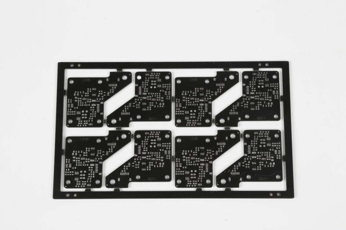
It is also known as characteristic panelization, in this process different types of printed circuit boards are combined together according to the combination principles. This process certainly has some good features. This process is suitable for production of such models which has combination of different types of printed circuit boards, for example households and some toys. It also contribute in terms increasing the production efficiency and cost cutting so that the products turnover and semi-finished products would not get piled up as inventory, and also makes it capable enough to meet the customer requirements of quick shipment. On the other hand it has some disadvantages as well. In the assembly line of printed circuit board, differentiation of products is difficult to manage, ultimately it cause chaos in the process. In the process of making combination if unfortunately one board is of good quality and another is of bad quality, then the overall number of such panelization will decreases and it bring down the manufacturing efficiency.
The ideal method of panelization is for production of a specific printed circuit board is decided through the manufacturing efficiency, process complexity, economy, the techniques of depanelization; of the process. The processes of depanelization are viz. V-groove and snap hole. In this process of depanelization, the pressure applied in the process is very critical. Hence it should be taken into full account , in order to restrict the deformation and also assurance regarding depanelization. The process of snap hole is generally utilized for printed circuit boards, whose thickness is less than 1 mm and consists with electronic components which are sensitive to external force like BGA so that the possibility of reflow deformation can be restricted. Ultimately the quality of product, improvement in efficiency of manufacturing process and distribution of external forces; such objectives can be achieved.
Panelization also offers a number of challenges. The method of depanelization produces lot of dust which is required to be vacuumed out. Laser cutting process must be used with board of thickness of 1 mm or less. The hanging part of printed circuit board must be managed, during the process of panelization possibility that these components can be damaged. Tolerances are also a critical consideration, if not defined well in initial design phase, then the cumulative effect of small variances in dimensions could cause abrupt failure. With more boards this problem usually get multiplied.
With the continuous development of the entire electronics industry, many products in the electronics industry have already established sophisticated upstream and downstream supporting enterprises. From a mature product design, design, manufacturing, assembly testing, packaging, wholesaler channels, etc., such an industrial chain is naturally generated in a specific environment. Therefore, the connection between design and manufacturing is extremely tight and in an inseparable position.
One of the most important aspects of electronic products from design completion to manufacturing is the processing of PCB boards. Most of the bare boards processed by the PCB are assembled by the placement machine.
Then the problem is coming, and now the electronic products are developing in the direction of small and light. When your design PCB board is particularly small, and some electronic product modules are as small as a few centimeters square, PCB manufacturing is better, but when it comes to prototype PCB assembly, a small area is placed on the placement machine for assembly. It brings problems. There is no way to assemble the production line!
Here, it is necessary to make a small PCB to be assembled into a suitable area that meets the requirements of the assembly machine, or to form a yin and yang board, which is more convenient for patch assembly. In general, the manufacturing board factory will provide the services of the panelization, but in the design of the AlTIum Designer software, in addition to more clearly showing the designer’s intention, there are many benefits, they are as follows:
1. Can be made in the direction you want.
2. The panelized file is associated with the source board, and the source board changes are automatically updated to the panelized board.
3. You can put together several different boards.
4. Can spell the yin and yang boards (reverse sides).
Here we use an example to introduce the process and operation steps of the panelization in AlTIum Designer.
Firstly,determine the size of the board. This can be viewed with Report > Board informaTIon. As shown in the figure below, this board is used as an example PCB board with a size of 75.18 x 30.23mm. We are going to spell a 2×2 PCB array in a new PCB.
Use File > New > PCB to create a rectangular PCB with a size of 160 x 65mm, 2 signal layers, no power plane, and vias. The newly created PCB for the panelization is as follows, saved.
On the newly created PCB, click Place > Embedded Board Array/Panelize. As shown below.
This is our jigsaw function. After entering it, you can see the following figure. Output the length and width in the Embedded Board Array window (this parameter is generally slightly larger than the original board. Depending on your needs). Select the board PCB file you want to spell in the PCB Document column. Then enter the number of horizontal and vertical rows to be spliced in the row and column element input boxes of the Column Count and Row Count.Each fill chooses 2.
After setting the above parameters, click OK to place the array board on the PCB. Adjust the position just right. And reposition the origin of the PCB to the origin of the array board.
Enter the level color manager below, rename Mechanical2 to Route Cutter Tool Layer, the line drawn on this layer is defined as the milling cutter milling PCB trace; the mechanical5 is renamed FabNotes, the line definition drawn on this layer In order to wash out the V-groove (V-GROOVE) trace on the PCB.
The following picture shows the array board with the detailed traces.
Note that we need to draw the Route Cutter Tool Layer traces and Fab Notes traces on the PCB array board. We need to let the processing board CAM drawing staff understand our specific needs and intentions. However, it is necessary to take the Cut or the V-slot, and the communication and communication between us and the board factory engineers shall prevail. Here is just a schematic.
Finally, it is to convert the PCB array board into a processing drawing file such as Gerber. Give the PCB processing board factory and communicate the specific process requirements and details with the board factory.
If any changes are made to the source PCB, these changes are updated in the PCB template file with one click. For example, in the figure below, place a pad in the source PCB.
Then in the PCB panelized file, click Refresh to refresh, and each of these boards will have such a pad. Update with the source board. As shown below.
Put together different PCBs, just select a PCB file and spell out the array. Then select another PCB file and then spell out the array. As shown below.
It should be noted here that for different PCBs to be put together, the number of layers and the thickness setting of the PCBs that need to be put together must be exactly the same. Can be put together for processing.
If you want to spell the yin and yang board, the method is to first use the panel function to place an array of boards, and then place another array of boards, then select the mirror. Similarly, the yin and yang boards must have the same thickness for each layer. Can be put together for processing.
Except altium panelize, if you want to know about easyeda panelize, eagle panelize, kicad panelize pcb , we will spend time to write a pcb panel guider about those software

Got project ready to assembly? Contact us: info@apollopcb.com


We're not around but we still want to hear from you! Leave us a note:

Leave Message to APOLLOPCB
