-
- PCB TYPE
- PRINTED CIRCUIT BOARD PROTOTYPE ALUMINUM PRINTED CIRCUIT BOARD R&F PCB FPC HIGH FREQUENCY PCB HIGH-TG PCB HEAVY COPPER PCB HDI PCB PCB FOR LIGHTING METAL CORE PCB
time:Jun 25. 2025, 09:40:23
In the ever - evolving landscape of lighting technology, Light - Emitting Diode (LED) model lights have emerged as a popular and efficient choice for a wide range of applications, from architectural lighting and display showcases to hobbyist projects. At the heart of these LED model lights lies the Aluminum Printed Circuit Board (Aluminum PCB), a crucial component that plays a pivotal role in determining the performance, reliability, and lifespan of the lighting system.
LEDs are known for their energy - efficiency, long - lifespan, and high - brightness output. However, they also generate a significant amount of heat during operation. If this heat is not effectively managed, it can lead to a decline in the LED's performance, reduced light output, and ultimately, a shorter lifespan. This is where aluminum PCBs come into play. Their unique properties make them an ideal solution for LED model lights, providing superior heat dissipation capabilities, mechanical robustness, and design flexibility.
This article delves deep into the world of LED model light aluminum PCBs. It explores their structure, advantages, design considerations, manufacturing processes, applications, and market trends. By understanding these aspects, lighting designers, manufacturers, and enthusiasts can make informed decisions when choosing and using aluminum PCBs for their LED model light projects, unlocking the full potential of this advanced technology.
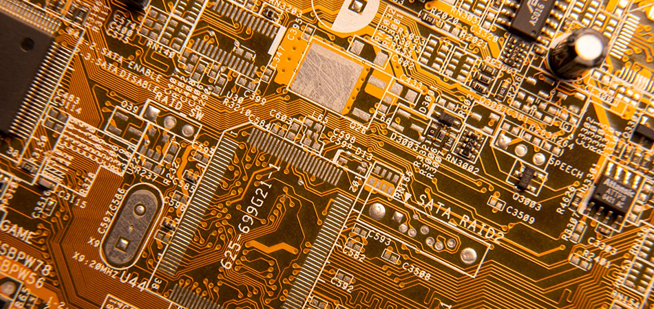
Structure of LED Model Light Aluminum PCBs
Layered Construction
LED model light aluminum PCBs typically feature a multi - layer construction, with each layer contributing to the overall functionality and performance of the board. The base layer is the aluminum substrate, which serves as the foundation for the entire structure. Aluminum is chosen for its excellent thermal conductivity, which allows it to efficiently transfer heat away from the LEDs. This not only helps to keep the LEDs cool but also improves their overall efficiency and lifespan.
On top of the aluminum substrate is the dielectric layer. This layer acts as an electrical insulator, preventing short - circuits between the conductive copper traces and the aluminum substrate. The dielectric material used in LED model light aluminum PCBs is carefully selected to have a high dielectric strength, good thermal stability, and low thermal resistance. Common dielectric materials include polyimide, epoxy - based resins, and thermally conductive polymers.
The outermost layer consists of the copper traces, which are patterned to form the electrical circuits that connect the LEDs and other components on the board. Copper is widely used for its high electrical conductivity, which ensures efficient transmission of electrical signals. The thickness and width of the copper traces are designed based on the current - carrying requirements of the LEDs, ensuring that they can handle the necessary power without overheating.
Material Selection
Aluminum Substrate
The choice of aluminum alloy for the substrate is crucial. Different aluminum alloys offer varying levels of thermal conductivity, mechanical strength, and corrosion resistance. For LED model lights, alloys with high thermal conductivity are preferred, as they can quickly dissipate the heat generated by the LEDs. Some commonly used aluminum alloys include 6061 and 5052. Alloy 6061, for example, has a good combination of strength and thermal conductivity, making it suitable for applications where the PCB may be subject to mechanical stress. Alloy 5052, on the other hand, offers excellent corrosion resistance, which is beneficial in environments where the LED model light may be exposed to moisture or other corrosive elementZ.
Dielectric Layer
The dielectric layer material must strike a balance between electrical insulation and thermal conductivity. Polyimide - based dielectrics are popular due to their high thermal stability, which allows them to withstand the elevated temperatures generated by the LEDs. They also have excellent electrical insulation properties, ensuring reliable operation of the electrical circuits. To further enhance the thermal conductivity of the dielectric layer, thermally conductive fillers such as aluminum oxide or boron nitride can be added. These fillers create a network within the dielectric material that facilitates the transfer of heat from the copper traces to the aluminum substrate.
Copper Traces
High - purity copper is used for the traces to maximize electrical conductivity. The thickness of the copper layer is determined by the current - carrying capacity required for the LEDs. Thicker copper layers can handle higher currents, but they also increase the cost and weight of the PCB. A common thickness for copper traces in LED model light aluminum PCBs is between 1 - 3 ounces per square foot. Additionally, the surface finish of the copper traces is important. Options such as electroless nickel immersion gold (ENIG), organic solderability preservative (OSP), and hot - air solder leveling (HASL) are available, each with its own advantages in terms of solderability, corrosion resistance, and electrical performance.
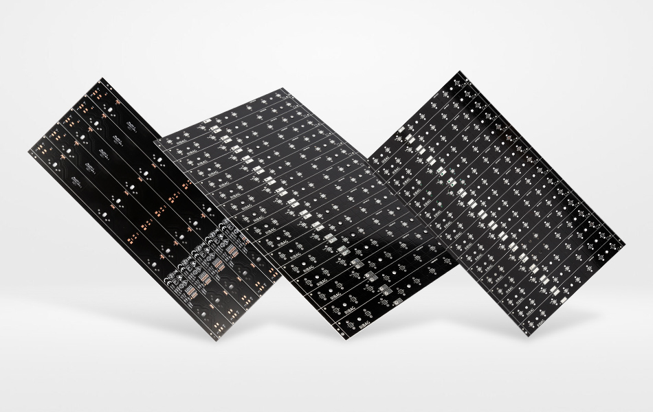
Advantages of Aluminum PCBs in LED Model Lights
Superior Heat Dissipation
One of the most significant advantages of using aluminum PCBs in LED model lights is their exceptional heat - dissipation capabilities. LEDs are highly sensitive to temperature, and even a small increase in operating temperature can lead to a significant decrease in light output and lifespan. The aluminum substrate in an aluminum PCB acts as a large - area heat sink, quickly absorbing the heat generated by the LEDs and distributing it across its surface. This rapid heat transfer helps to keep the LEDs operating at a lower and more stable temperature, ensuring consistent light output and a longer lifespan.
For example, in a high - brightness LED model light used for architectural lighting, the heat generated by the LEDs can be substantial. Without proper heat management, the LEDs may overheat, resulting in a dimmer light output and a shorter lifespan. By using an aluminum PCB, the heat is efficiently dissipated, allowing the LEDs to operate at their optimal performance level. This not only improves the quality of the lighting but also reduces the need for additional cooling mechanisms, such as fans or heat sinks, which can add to the complexity and cost of the lighting system.
Mechanical Robustness
LED model lights are often used in various environments, some of which may be subject to mechanical stress, vibration, or shock. Aluminum PCBs offer excellent mechanical strength and durability, making them suitable for such applications. The aluminum substrate provides a rigid and stable base for the PCB, protecting the delicate electrical components from damage. This mechanical robustness is particularly important in applications where the LED model light may be moved or transported frequently, such as in exhibition displays or portable lighting setups.
In addition, the multi - layer construction of aluminum PCBs further enhances their mechanical strength. The layers are bonded together using high - temperature and high - pressure processes, creating a strong and cohesive structure. This makes the PCB resistant to bending, cracking, and other forms of mechanical damage, ensuring its reliable operation over an extended period.
Design Flexibility
Aluminum PCBs offer a high degree of design flexibility, allowing lighting designers to create innovative and customized LED model light solutions. The ability to pattern the copper traces in intricate designs enables the integration of multiple LEDs, drivers, and other components on a single board. This not only reduces the overall size and complexity of the lighting system but also improves its performance by minimizing the length of the electrical connections.
Furthermore, the aluminum substrate can be easily shaped and formed to fit specific design requirements. It can be bent, curved, or cut into various shapes, making it suitable for use in LED model lights with unique form factors. For example, in a curved LED strip used for accent lighting, the aluminum PCB can be fabricated to match the curvature of the strip, providing a seamless and visually appealing lighting solution.
Cost - Effectiveness in the Long Run
Although the initial cost of aluminum PCBs may be higher compared to some traditional PCBs, they offer significant long - term cost - savings in LED model light applications. Their superior heat - dissipation capabilities reduce the need for additional cooling components, which can be costly to purchase and install. By efficiently managing the heat generated by the LEDs, aluminum PCBs also extend the lifespan of the LEDs, reducing the frequency of replacements and maintenance.
In addition, the mechanical robustness of aluminum PCBs means that they are less likely to be damaged during handling or operation. This reduces the risk of costly repairs or replacements, further contributing to the overall cost - effectiveness of the lighting system. Over the long term, the use of aluminum PCBs in LED model lights can result in substantial savings in both energy consumption and maintenance costs.
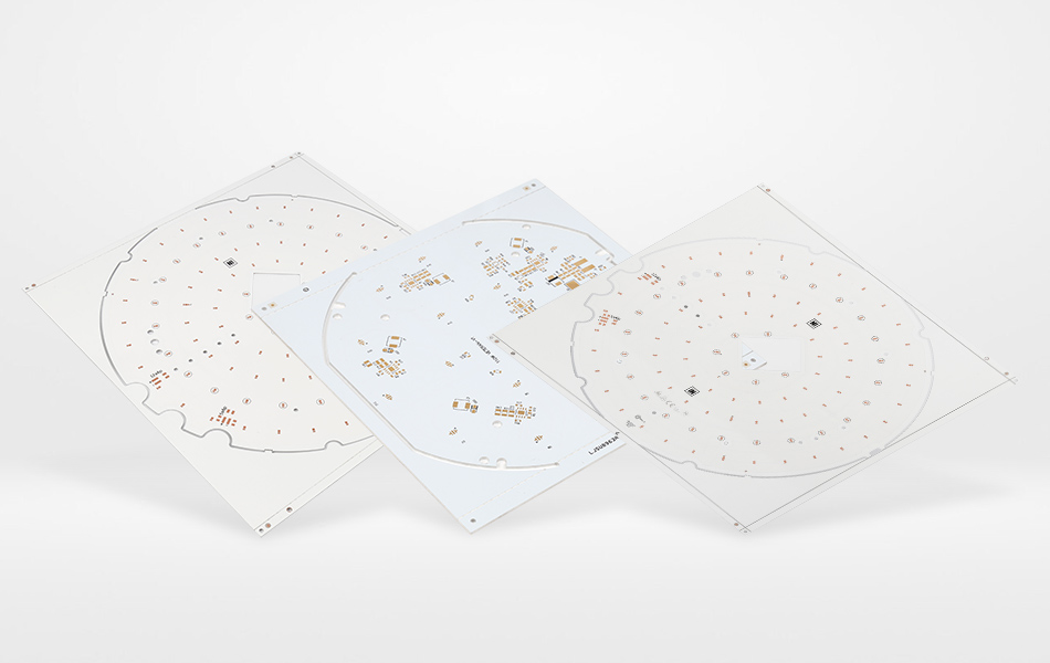
Design Considerations for LED Model Light Aluminum PCBs
Thermal Design
LED Placement
Proper placement of the LEDs on the aluminum PCB is crucial for effective heat dissipation. LEDs should be positioned in a way that maximizes their contact with the aluminum substrate. This can be achieved by placing them directly on the substrate or using thermal vias to connect them to the substrate. Thermal vias are small holes filled with a conductive material, such as copper, that facilitate the transfer of heat from the LEDs to the aluminum substrate.
In addition, the layout of the LEDs should be carefully planned to ensure even heat distribution across the board. Clustering the LEDs too closely together can lead to hotspots, where the heat accumulates and causes the LEDs to overheat. By spreading the LEDs out evenly, the heat can be more effectively dissipated, ensuring consistent performance across all the LEDs.
Thermal Via Design
The design of thermal vias is a critical aspect of thermal management in LED model light aluminum PCBs. The size, number, and distribution of thermal vias should be optimized based on the heat - generation characteristics of the LEDs and the thermal conductivity of the materials used in the PCB. Larger thermal vias can transfer more heat, but they also take up more space on the board. Therefore, a balance must be struck between heat - transfer efficiency and space utilization.
The number of thermal vias should be sufficient to handle the heat generated by the LEDs. This can be determined through thermal simulation software, which can analyze the heat flow within the PCB and predict the temperature distribution. Based on the simulation results, the number and location of thermal vias can be adjusted to ensure optimal heat dissipation.
Heat - Sink Integration
In some cases, integrating a heat sink with the aluminum PCB can further enhance heat dissipation, especially for high - power LED model lights. The heat sink provides an additional surface area for heat dissipation, allowing the LEDs to operate at even lower temperatures. When integrating a heat sink, it is important to ensure good thermal contact between the heat sink and the aluminum substrate. This can be achieved using thermal interface materials, such as thermal paste or pads, which fill the gaps between the two surfaces and improve heat transfer.
The design of the heat sink, including its size, shape, and fin configuration, should be tailored to the specific heat - dissipation requirements of the LED model light. A well - designed heat sink can significantly improve the performance and lifespan of the LEDs, but it also needs to be carefully integrated into the overall design of the lighting system to ensure compatibility and aesthetics.
Electrical Design
Trace Routing
Trace routing in LED model light aluminum PCBs must be carefully planned to ensure reliable electrical performance. The copper traces should be routed in a way that minimizes resistance, inductance, and capacitance. This is particularly important for high - current applications, where even a small increase in resistance can lead to significant power losses and heat generation.
To minimize resistance, the traces should be as short and wide as possible. The width of the traces should be sufficient to carry the current required by the LEDs without overheating. In addition, the traces should be routed in a straight line whenever possible, avoiding sharp corners or bends, which can increase inductance.
Power and Ground Plane Design
Proper power and ground plane design is essential for stable power distribution and reduced electromagnetic interference (EMI) in LED model light aluminum PCBs. The power plane should be designed to provide a low - impedance path for the power supply to the LEDs, ensuring a stable and consistent voltage. The ground plane, on the other hand, serves as a reference point for the electrical circuits and helps to reduce EMI by providing a return path for the current.
To minimize voltage drops and improve power distribution, the power and ground planes should be as large as possible. They should also be separated from each other to prevent electrical interference. In addition, decoupling capacitors should be placed near the LEDs and other components to filter out high - frequency noise and ensure stable power supply.
Design for Manufacturability
Design for manufacturability (DFM) is an important consideration when designing LED model light aluminum PCBs. DFM principles aim to simplify the manufacturing process, reduce costs, and improve the quality and reliability of the final product. This includes using standard component footprints, avoiding complex shapes and geometries, and ensuring compatibility with manufacturing processes.
Using standard component footprints makes it easier to source components and reduces the risk of errors during assembly. Avoiding complex shapes and geometries, such as sharp corners or narrow slots, simplifies the fabrication process and reduces the likelihood of manufacturing defects. In addition, the design should be compatible with the manufacturing processes used, such as drilling, plating, and soldering, to ensure that the PCB can be produced efficiently and cost - effectively.
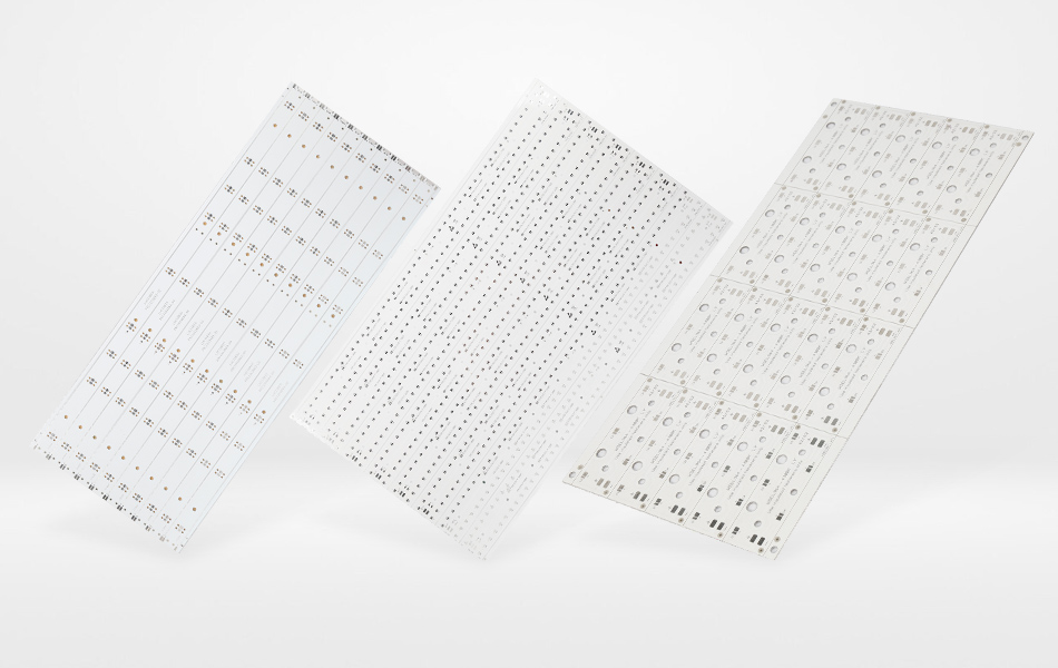
Manufacturing Processes of LED Model Light Aluminum PCBs
Material Preparation
The manufacturing process of LED model light aluminum PCBs begins with the careful selection and preparation of materials. High - quality aluminum sheets are chosen based on their thermal conductivity, mechanical properties, and surface finish. These sheets are then cut to the required size and shape for the substrate.
The dielectric material, which is typically in the form of a pre - impregnated film or a liquid resin, is also prepared. Pre - impregnated films are made by impregnating a base material, such as fiberglass, with a thermosetting resin. The film is then cured to a semi - cured state, known as a B - stage, which allows it to be easily handled and laminated. Liquid resins, on the other hand, are mixed with fillers and other additives to achieve the desired properties, such as high thermal conductivity and good electrical insulation.
High - purity copper foils are selected for the traces. These foils are cleaned and treated to improve their adhesion to the dielectric layer. The thickness of the copper foils is carefully controlled to meet the current - carrying requirements of the LEDs.
Lamination
Lamination is the process of bonding the aluminum substrate, dielectric layer, and copper foils together to form a single, cohesive structure. This is typically done using heat and pressure in a laminator. The heat activates the thermosetting resin in the dielectric layer, causing it to flow and bond with the aluminum substrate and copper foils. The pressure ensures that the layers are in intimate contact with each other, eliminating any air gaps or voids that could affect the performance of the PCB.
The lamination process requires precise control of temperature, pressure, and time to ensure a high - quality bond. Different laminators may use different techniques, such as vacuum lamination or press lamination, depending on the specific requirements of the PCB. After lamination, the PCB is cooled and trimmed to the final size.
Drilling and Plating
Once the PCB is laminated, holes are drilled for vias, component mounting, and electrical connections. High - precision drilling machines are used to ensure accurate hole placement and clean hole walls. The holes are then plated with copper to create electrical connections between the different layers of the PCB.
Electroplating is the most common method used for copper plating. In this process, the PCB is immersed in an electrolyte solution containing copper ions. An electric current is applied, causing the copper ions to deposit on the surface of the holes and the copper traces. The thickness of the copper plating is carefully controlled to ensure proper electrical conductivity and mechanical strength.
Circuit Patterning
Circuit patterning is the process of creating the electrical circuits on the copper layers of the PCB. This is typically done using photolithography, a technique that involves exposing a photosensitive resist to ultraviolet (UV) light through a patterned mask. The areas of the resist that are exposed to the UV light are then removed using a developer solution, leaving behind the desired circuit pattern.
The remaining copper areas are then etched away using an etching solution, such as ferric chloride or ammonium persulfate. This leaves behind the copper traces that form the electrical circuits. The circuit patterning process requires high precision to ensure accurate trace widths, clearances, and the absence of shorts or open circuits.
Surface Finish
The final step in the manufacturing process of LED model light aluminum PCBs is the application of a surface finish. The surface finish serves several purposes, including protecting the copper traces from corrosion, improving solderability, and enhancing the appearance of the PCB.
Common surface finishes for aluminum PCBs include electroless nickel immersion gold (ENIG), organic solderability preservative (OSP), and hot - air solder leveling (HASL). ENIG provides a smooth and corrosion - resistant surface that is highly solderable. OSP is a thin, organic coating that protects the copper from oxidation and provides good solderability. HASL involves dipping the PCB in a bath of molten solder, which coats the copper traces with a layer of solder.
Applications of LED Model Light Aluminum PCBs
Architectural Lighting
LED model light aluminum PCBs are widely used in architectural lighting applications, where they offer a combination of high - performance lighting and design flexibility. In buildings, they can be used for general illumination, accent lighting, and decorative lighting. For example, in a lobby or entrance area, aluminum - PCB - based LED model lights can be used to create a warm and inviting atmosphere. The ability to control the color, intensity, and direction of the light allows for the creation of unique lighting effects that enhance the architectural features of the space.
In addition, the energy - efficiency and long - lifespan of LED model lights with aluminum PCBs make them a sustainable choice for architectural lighting. They consume less energy compared to traditional lighting sources, reducing the building's energy consumption and operating costs. Their long lifespan also means that they require less frequent maintenance and replacement, minimizing disruption to the building occupants.
Display Showcases
LED model light aluminum PCBs are ideal for display showcases, such as those used in museums, art galleries, and retail stores. In these applications, the lighting needs to be carefully controlled to highlight the exhibits or products while minimizing glare and heat. Aluminum PCBs provide excellent heat dissipation, ensuring that the LEDs do not overheat and damage the delicate items on display.
The high - brightness and color - rendering capabilities of LEDs on aluminum PCBs also make them suitable for accurately presenting the colors and details of the exhibits. The ability to customize the lighting design, such as using different color temperatures or creating specific lighting patterns, allows for a more engaging and immersive display experience for the viewers.

Got project ready to assembly? Contact us: info@apollopcb.com


We're not around but we still want to hear from you! Leave us a note:

Leave Message to APOLLOPCB
