-
- PCB TYPE
- PRINTED CIRCUIT BOARD PROTOTYPE ALUMINUM PRINTED CIRCUIT BOARD R&F PCB FPC HIGH FREQUENCY PCB HIGH-TG PCB HEAVY COPPER PCB HDI PCB PCB FOR LIGHTING METAL CORE PCB
time:Oct 21. 2025, 09:58:08
Printed Circuit Boards (PCBs) are the backbone of modern electronic devices. From smartphones to kitchen appliances, they are integral to the functioning of countless gadgets. But how are these vital components made? In this article, we'll explore the PCB assembly process, breaking down the steps involved in transforming a custom PCB design into a working product.
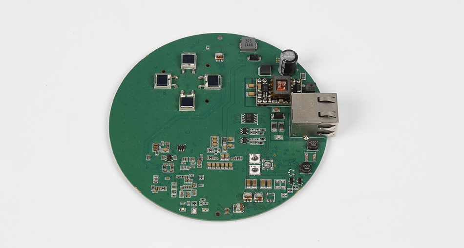
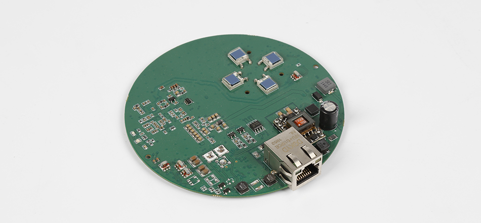
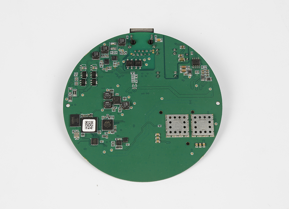
PCB assembly, often abbreviated as PCBA, is the process of soldering electronic components onto a printed circuit board. This assembly transforms the board from a simple substrate into a complex electronic circuit capable of performing specific functions. Whether you're dealing with a custom PCB or a standard design, the assembly process is crucial to ensuring the board functions correctly.

The journey of a PCB begins with a design. Engineers use specialized software to create a schematic of the circuit, laying out where each component will go and how they will connect. Once the design is complete, a prototype is often created. This prototype helps in identifying any potential issues before the full-scale PCB manufacturing begins.
Importance of Prototyping
Prototyping is a vital step in PCB assembly. It allows designers to test and refine their designs, ensuring the final product is free from errors. This stage can save both time and money by catching mistakes early on.
After the design phase, the next step is the physical creation of the PCB. This process involves several stages, including:
Printing the Design: The PCB design is printed onto a laminate material, often using a laser printer. This printed design acts as a blueprint for the rest of the manufacturing process.
Etching: Once printed, the board undergoes etching. This removes any unwanted copper, leaving behind only the desired circuit pattern.
Drilling: Holes are drilled into the board to accommodate components' leads and vias, which are pathways for electrical connections between layers.
Plating: A thin layer of copper is applied to the drilled holes, creating conductive paths through the board.
Solder Mask Application: A solder mask is applied to protect the copper traces and prevent short circuits. This mask gives PCBs their characteristic green color.
Silkscreen Printing: Finally, a silkscreen is applied, adding labels and markings to the board for easy identification of components and connections.

With the board manufactured, the next step is placing the components onto it. This process can be done manually or automatically using machines. Automated placement is preferred for larger production runs due to its speed and precision.
Surface Mount Technology (SMT)
SMT is a popular method for placing components onto a PCB. It involves placing components directly onto the surface of the board, rather than inserting them through holes. SMT allows for more compact designs and is ideal for high-density circuits.
Once the components are in place, they need to be soldered to the board. Soldering creates a permanent electrical connection between the components and the PCB. There are two main methods of soldering:
Reflow Soldering: Used primarily with SMT, this method involves applying solder paste to the board, placing the components, and then passing the board through an oven. The heat melts the solder, forming connections.
Wave Soldering: Used for through-hole components, this method involves passing the board over a wave of molten solder, which coats the exposed metal surfaces, forming connections.
After soldering, the PCB undergoes inspection and testing to ensure it's functioning correctly. This step is critical for identifying defects or errors before the board is shipped or integrated into a larger product.
Common Testing Methods
Visual Inspection: Checking for obvious defects such as misaligned components or solder bridges.
Automated Optical Inspection (AOI): Using cameras to automatically inspect the board for defects.
Functional Testing: Testing the board under real-world conditions to ensure it performs as expected.
Once tested, the PCB is ready for final assembly. This involves integrating the PCB into its final product, whether it's a smartphone, computer, or other electronic device. The final assembly process may also include adding enclosures, connectors, and other necessary components.

The PCB assembly process is a complex series of steps that transform a simple board into a fully functional electronic circuit. From the initial design and prototyping to the final assembly, each stage is critical to ensuring the quality and functionality of the finished product. Whether you're working with a custom PCB or a standard design, understanding this process can help you appreciate the intricate work that goes into every electronic device.
By understanding the PCB assembly process, you gain insight into the backbone of modern technology, and how these essential components are brought to life. Whether you're a hobbyist or an industry professional, this knowledge is invaluable in the ever-evolving world of electronics.

Got project ready to assembly? Contact us: info@apollopcb.com


We're not around but we still want to hear from you! Leave us a note:

Leave Message to APOLLOPCB
