-
- PCB TYPE
- PRINTED CIRCUIT BOARD PROTOTYPE ALUMINUM PRINTED CIRCUIT BOARD R&F PCB FPC HIGH FREQUENCY PCB HIGH-TG PCB HEAVY COPPER PCB HDI PCB PCB FOR LIGHTING METAL CORE PCB
time:Jul 02. 2025, 15:37:25
In the ever-evolving realm of radio frequency (RF) technology, the demand for advanced printed circuit boards (PCBs) has reached unprecedented heights. RF applications, spanning from 5G wireless networks to aerospace radar systems, impose rigorous demands on PCB design, particularly in signal integrity, thermal management, and durability. Among the innovative solutions, aluminum-based PCBs (Al PCBs) integrated with blind vias have emerged as a pivotal technology to address these challenges. This article explores the technical intricacies, operational advantages, and practical considerations of incorporating blind vias into Al PCBs for RF applications, highlighting how this combination revolutionizes performance and reliability in high-frequency environments.
The Evolution of RF Technology and PCB Demands
The Expanding Scope of RF Applications
RF technology has become the backbone of modern connectivity, powering diverse sectors such as telecommunications, automotive electronics, and satellite communications. The deployment of 5G networks, for instance, requires PCBs that can handle frequencies up to millimeter-wave ranges, demanding precise signal control and minimal loss. Similarly, automotive radar systems operating at 77 GHz or higher necessitate PCBs that maintain signal fidelity while withstanding harsh environmental conditions. These advancements have propelled the need for PCBs that balance high-frequency performance with robust thermal and mechanical properties.
Core Challenges in RF PCB Design
Designing PCBs for RF applications presents unique hurdles. At high frequencies, signal degradation due to dielectric loss and impedance mismatching becomes critical. Electromagnetic interference (EMI) and crosstalk pose significant risks, as even minor disturbances can compromise system functionality. Thermal management is equally challenging, as RF components like power amplifiers generate substantial heat, which if not dissipated efficiently, can lead to thermal runaway and component failure. Additionally, reliability under varying temperatures, vibrations, and humidity levels is non-negotiable for applications in aerospace, automotive, and industrial sectors.
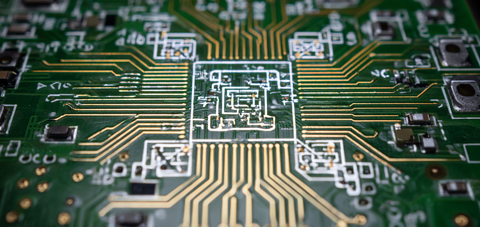
Blind Vias: A Technical Perspective for RF Applications
Defining Blind Vias and Their Functionalities
Blind vias are conductive pathways that connect the outer layer of a PCB to one or more inner layers without penetrating the entire board. Unlike through-hole vias, they offer localized connectivity, making them ideal for complex multi-layer designs. In RF PCBs, blind vias are typically classified by their depth and placement, such as single-sided blind vias (connecting top layer to an inner layer) or buried vias (connecting inner layers without reaching the surface). Their precise design allows for controlled signal routing, essential in high-frequency environments.
Advantages of Blind Vias in RF Circuits
Superior Signal Integrity: By reducing via length, blind vias minimize signal delay and phase distortion, crucial for maintaining waveform accuracy in RF signals. The shorter path also decreases inductance and capacitance, lowering signal loss and improving return loss performance.
EMI Mitigation: The localized nature of blind vias reduces electromagnetic radiation, preventing interference with adjacent traces. This is particularly vital in dense RF layouts where multiple high-frequency signals coexist.
Compact Design Efficiency: Blind vias enable more efficient use of board space by eliminating the need for through-hole vias, which require clearance on both sides. This compactness is essential for portable RF devices and systems with strict size constraints.
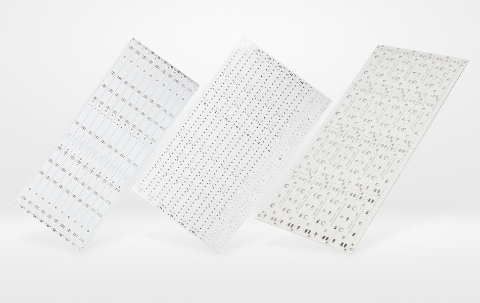
Aluminum-Based PCBs: Thermal and Mechanical Advantages
Properties of Aluminum Substrates in PCBs
Al PCBs feature a metal core (typically aluminum) sandwiched between dielectric layers and conductive traces. The aluminum core offers exceptional thermal conductivity (approximately 200-240 W/mK), far exceeding that of traditional fiberglass substrates (e.g., FR-4, ~0.25 W/mK). This property allows Al PCBs to dissipate heat rapidly, making them suitable for high-power RF applications. Additionally, aluminum provides mechanical rigidity, enhancing the board’s resistance to physical stress and vibration.
Thermal Management in RF Systems
In RF applications, efficient thermal management is non-negotiable. Excessive heat can alter component characteristics, such as increasing resistance in traces or degrading semiconductor performance. Al PCBs address this by acting as a heat sink, distributing heat from high-power components (e.g., RF amplifiers) across the aluminum core. This reduces thermal gradients and hotspots, maintaining consistent operating temperatures and extending component lifespan. For example, in base station antennas, Al PCBs enable continuous high-power transmission without performance degradation due to overheating.
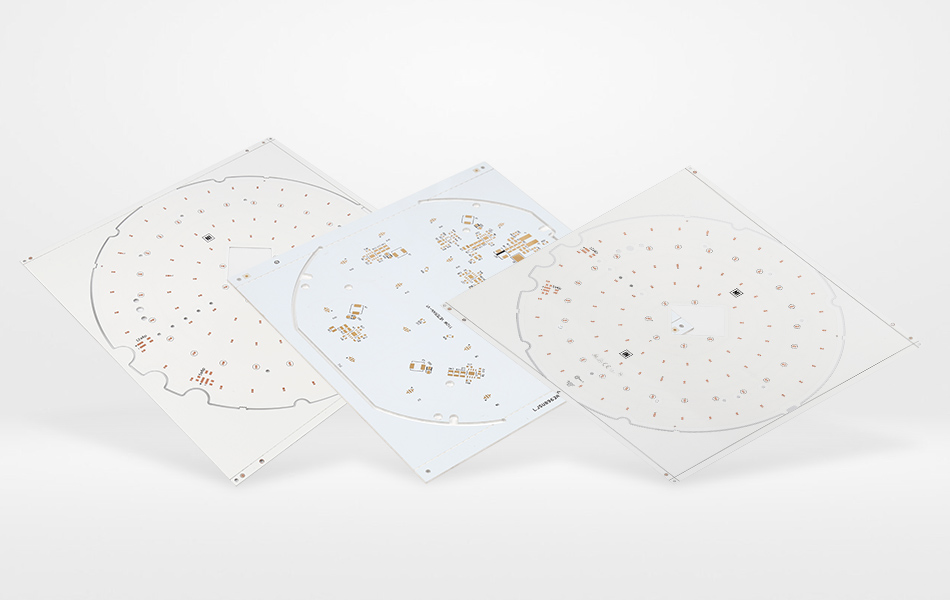
The Synergy of Blind Vias and Al PCBs in RF Applications
Enhancing Signal Integrity Through Combined Design
The integration of blind vias with Al PCBs creates a synergistic effect in RF systems. The low-loss dielectric materials used in Al PCBs (e.g., ceramic-filled polymers or PTFE composites) complement blind via design by minimizing signal attenuation. Additionally, the thermal stability of aluminum cores prevents temperature-induced changes in dielectric constants, ensuring consistent impedance control—a critical factor in maintaining signal integrity at high frequencies.
Thermal Via Optimization for Heat Dissipation
Blind vias can be strategically designed as thermal vias to enhance heat transfer in Al PCBs. By placing vias beneath high-heat components, heat is conducted from the surface layers to the aluminum core more efficiently. Filling these vias with thermally conductive materials (e.g., silver-loaded epoxy) further improves thermal conductivity, creating a direct pathway for heat dissipation. This technique is particularly effective in RF power amplifiers, where managing junction temperatures is essential for maintaining gain and linearity.
Reliability Improvements in Harsh Environments
Al PCBs with blind vias exhibit superior reliability in challenging environments. The aluminum core reduces thermal stress on the PCB, minimizing the risk of delamination or cracking caused by repeated thermal cycling. Furthermore, the mechanical strength of aluminum protects the board from vibration-induced damage, making it suitable for automotive radar systems or aerospace applications. The combination of these features ensures long-term performance stability in extreme temperatures and dynamic conditions.
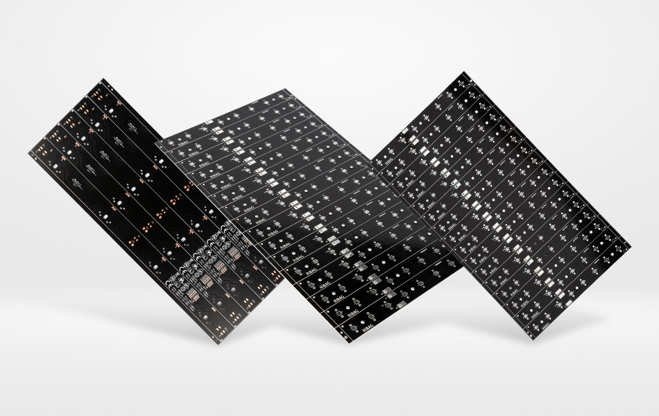
Design Considerations for RF Al PCBs with Blind Vias
Material Selection for Optimal Performance
Dielectric Materials: Choose low-loss dielectrics with stable permittivity (Dk) and low tangent delta (Df) across the RF frequency range. Common choices include PTFE-based materials (e.g., Rogers RO3000 series) or ceramic-filled laminates, which balance signal integrity with thermal compatibility with aluminum cores.
Aluminum Core Thickness: The core thickness affects thermal conductivity and mechanical rigidity. Thicker cores (e.g., 100-200 µm) offer better thermal performance but may increase board weight, while thinner cores (e.g., 50 µm) are suitable for space-constrained designs.
Blind Via Design Parameters
Via Diameter and Depth: Optimize via dimensions to balance electrical and thermal performance. Smaller vias (e.g., 50-100 µm) are suitable for dense layouts but may have higher resistance, while larger vias (e.g., 150-200 µm) improve conductivity but require more space.
Aspect Ratio: Maintain a reasonable aspect ratio (via depth to diameter) to ensure uniform plating. A ratio of 3:1 or lower is ideal for reliable via conductivity, especially in multi-layer boards.
Placement Strategy: Avoid placing blind vias near critical RF traces to minimize interference. Instead, position them beneath heat-generating components or along ground planes to enhance thermal dissipation and EMI shielding.
Manufacturing Processes for Precision
Laser Drilling: For small blind vias, laser drilling offers high precision and minimal material damage, ensuring accurate via depth control. CO2 or UV lasers are commonly used for dielectric materials, while fiber lasers may be suitable for metalized layers.
Electroless and Electrolytic Plating: A two-step plating process ensures uniform copper deposition within vias, preventing voids or thin spots that could compromise conductivity. Post-plating via filling with thermally conductive materials further enhances reliability.
Thermal Compatibility Testing: During manufacturing, validate the thermal compatibility between aluminum cores and dielectric layers to prevent delamination. Processes like controlled impedance lamination and post-bond cure cycles are essential for maintaining structural integrity.
Testing and Quality Assurance Protocols
Electrical Performance Validation
Vector Network Analysis (VNA): Measure key parameters such as insertion loss (S21), return loss (S11), and crosstalk (S31) across the operational frequency band. VNAs help identify impedance mismatches or signal degradation caused by via design or material selection.
Time-Domain Reflectometry (TDR): Evaluate signal integrity by analyzing how signals propagate through the PCB, detecting discontinuities in traces or vias that may cause reflections.
Thermal Performance Testing
Infrared (IR) Thermography: Monitor temperature distributions on the PCB under simulated RF operating conditions. This identifies hotspots and evaluates the effectiveness of thermal via design and aluminum core heat dissipation.
Thermal Cycling Tests: Subject the PCB to repeated temperature cycles (e.g., -40°C to +125°C) to assess its durability and resistance to thermal stress. Changes in electrical performance or physical defects (e.g., cracks) are monitored to ensure long-term reliability.
Environmental Reliability Testing
Humidity and Temperature Resistance: Perform tests like 85°C/85% RH for 1000 hours to evaluate the PCB’s resistance to moisture-induced degradation, crucial for outdoor RF applications.
Vibration and Shock Testing: Simulate mechanical stresses encountered in automotive or aerospace environments to ensure the PCB remains functional without component detachment or via cracking.
Emerging Trends and Future Innovations
Advanced Materials for Next-Generation RF PCBs
The development of new dielectric materials with even lower loss and better thermal conductivity is ongoing. For example, ceramic-polymer composites and nanomaterial-enhanced dielectrics aim to further reduce Df and improve thermal management in Al PCBs. Additionally, advancements in aluminum core surface treatments (e.g., anodization) may enhance adhesion with dielectric layers, enabling thinner and more reliable designs.
3D Packaging and Heterogeneous Integration
As RF systems become more complex, 3D packaging techniques that integrate multiple components (e.g., antennas, amplifiers, and filters) on a single Al PCB with blind vias are gaining traction. This approach minimizes signal path lengths, improves system integration, and reduces overall size—critical for applications like mmWave 5G modules and compact radar systems.
AI-Driven Design Optimization
Artificial intelligence and machine learning algorithms are being applied to optimize blind via placement and Al PCB design for RF applications. These tools can simulate various design scenarios, predict thermal and electrical performance, and recommend optimal parameters to balance performance, cost, and reliability—a trend that will likely accelerate in the coming years.
Conclusion
The integration of blind vias into aluminum-based PCBs represents a significant advancement in RF technology, addressing the critical challenges of signal integrity, thermal management, and reliability. By leveraging the unique properties of aluminum cores and the precision of blind via design, engineers can create RF PCBs that excel in high-frequency, high-power environments. As RF applications continue to push the boundaries of frequency, bandwidth, and miniaturization, the synergy of Al PCBs and blind vias will remain essential for driving innovation in wireless communication, radar, and beyond. Through ongoing material advancements, manufacturing refinements, and design optimizations, this technology will continue to enhance the performance and reliability of next-generation RF systems.

Got project ready to assembly? Contact us: info@apollopcb.com


We're not around but we still want to hear from you! Leave us a note:

Leave Message to APOLLOPCB
