-
- PCB TYPE
- PRINTED CIRCUIT BOARD PROTOTYPE ALUMINUM PRINTED CIRCUIT BOARD R&F PCB FPC HIGH FREQUENCY PCB HIGH-TG PCB HEAVY COPPER PCB HDI PCB PCB FOR LIGHTING METAL CORE PCB
time:Nov 07. 2025, 10:28:50
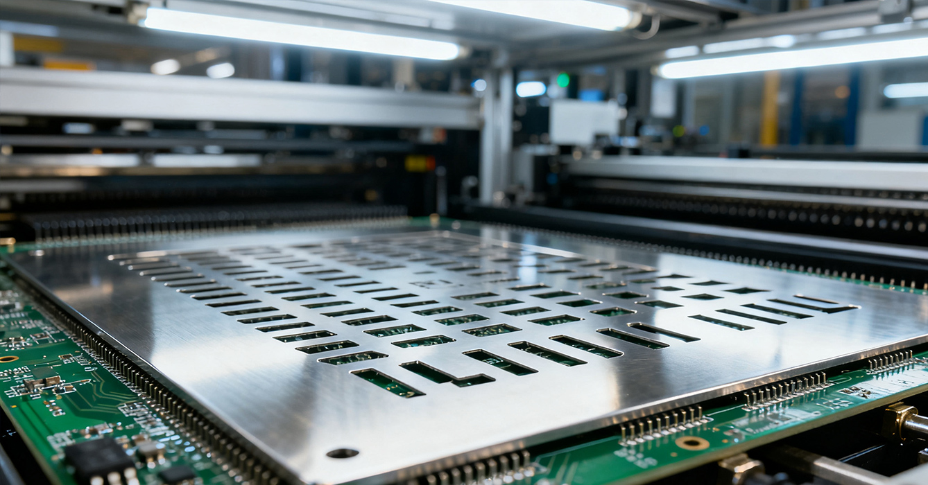
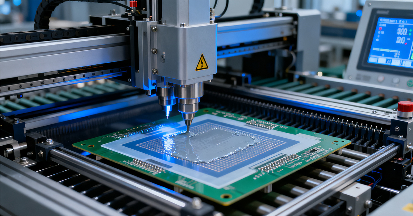
SMT Stencils are the foundational component of surface-mount technology (SMT) assembly, serving as the precision tool that deposits solder paste onto printed circuit boards (PCBs) to create electrical connections between components and pads. Often overlooked amid more complex assembly equipment, these thin, metal sheets play a make-or-break role in determining product quality—even minor flaws in stencil design or fabrication can lead to costly defects like solder bridging, insufficient paste, or tombstoning. As electronics evolve toward miniaturization, higher component density, and faster production cycles, the role of SMT stencils has grown from a simple "template" to a technically advanced solution that aligns with the demands of modern manufacturing. This article explores the technical evolution of SMT stencils, critical quality factors that define their performance, their impact on assembly efficiency, and how they adapt to emerging electronics trends.

SMT stencils have undergone significant innovation to keep pace with advancing PCB designs, with three key generations of technology:
- Chemical Etching: The earliest mainstream method, ideal for simple, low-density PCBs. Chemical etching uses acidic solutions to create apertures, offering cost-effectiveness for basic designs but limited precision for fine-pitch components.
- Laser Cutting: A mid-2000s breakthrough that revolutionized stencil precision. Fiber lasers ablate metal to create clean, consistent apertures with tight tolerances, making it suitable for fine-pitch ICs (down to 0.4mm pitch) and mixed-component boards. It remains the most widely used method today due to its balance of speed, accuracy, and cost.
- Electroforming: The latest advancement, designed for ultra-miniaturized components (e.g., 01005 passives, microLEDs). Electroforming deposits nickel layer-by-layer onto a precision master, creating apertures with smooth sidewalls and sub-micron accuracy—critical for ensuring reliable paste transfer in high-density HDI PCBs.

title="3-2" alt="3-2"/>
The performance of SMT stencils hinges on three non-negotiable quality pillars, none of which rely on specific product parameters:
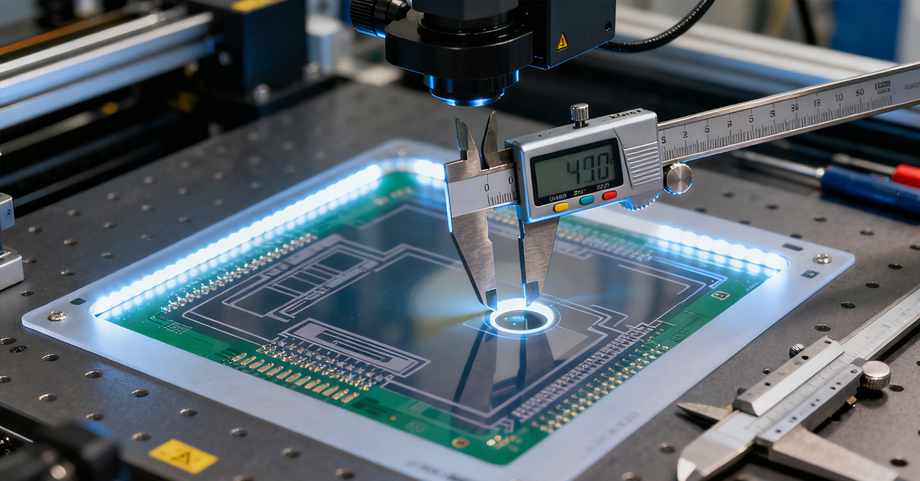
Apertures must match PCB pad dimensions exactly, with uniform edge quality to prevent solder buildup or uneven release. Even slight variations in aperture size (e.g., +/−5 microns) can cause under-soldering or bridging, especially for small components. Stencil manufacturers use optical measurement systems to validate aperture consistency across the entire stencil.
High-quality stencils use corrosion-resistant stainless steel to withstand repeated cleaning and printing cycles. Surface treatments further enhance performance: nano-coatings reduce solder paste adhesion, extending stencil lifespan and reducing downtime for cleaning; electropolishing smooths aperture edges to improve paste release efficiency.
Stencils must maintain consistent tension when mounted on printers to avoid warping during printing. A warped stencil can misalign apertures with PCB pads, leading to defects. Manufacturers use specialized framing equipment to ensure flatness and uniform tension, critical for high-volume production runs.

Well-designed SMT stencils are a catalyst for assembly efficiency, driving three key improvements:
- Reduced Defect Rates: Precise apertures and smooth paste release cut defect rates by up to 50% compared to low-quality stencils, minimizing rework time and material waste.
- Faster Production Cycles: Stencils with optimized surface treatments require less frequent cleaning, extending time between production stops and increasing line throughput.
- Lower Total Cost of Ownership: Durable materials and treatments extend stencil lifespan (from thousands to tens of thousands of prints), reducing the frequency of stencil replacements and lowering long-term costs.

SMT stencils are evolving to meet two key industry trends:
As components shrink to sub-millimeter sizes, stencil manufacturers are developing electroformed stencils with apertures as small as 50 microns. Advanced laser systems with shorter wavelengths also enable tighter aperture spacing for dense PCBs in smartphones and wearables.
The industry is shifting toward eco-friendly practices: recyclable stainless steel reduces material waste, while water-based cleaning agents for stencils replace solvent-based alternatives. Manufacturers are also exploring reusable stencil frames to minimize packaging waste.
SMT Stencils may be unconspicuous, but they are the backbone of reliable, efficient electronics assembly. Their technical evolution—from chemical etching to electroforming—mirrors the advancement of electronics themselves, while strict quality controls ensure they meet the demands of modern manufacturing. As components grow smaller and sustainability becomes a priority, SMT stencils will continue to innovate, proving that even the "simplest" tools are critical to unlocking the next generation of electronic devices. For manufacturers, investing in high-quality SMT stencils is not just a production choice—it’s an investment in consistent quality and long-term efficiency.

Got project ready to assembly? Contact us: info@apollopcb.com


We're not around but we still want to hear from you! Leave us a note:

Leave Message to APOLLOPCB
