-
- PCB TYPE
- PRINTED CIRCUIT BOARD PROTOTYPE ALUMINUM PRINTED CIRCUIT BOARD R&F PCB FPC HIGH FREQUENCY PCB HIGH-TG PCB HEAVY COPPER PCB HDI PCB PCB FOR LIGHTING METAL CORE PCB
time:Nov 17. 2025, 12:47:24
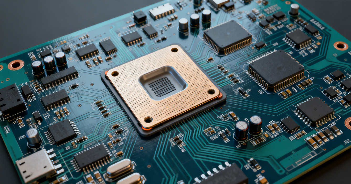
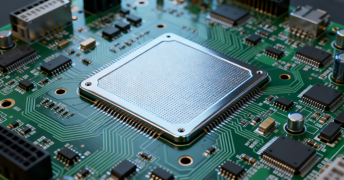
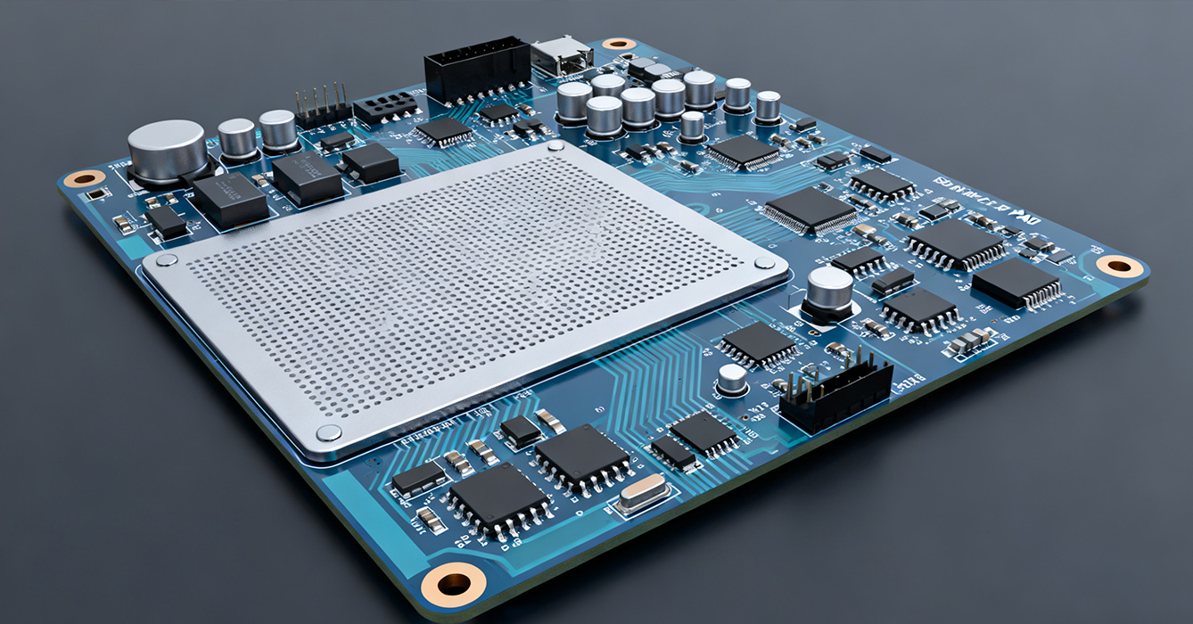
Sinkpad PCB has emerged as a critical enabler for next-generation electronic systems, addressing the growing demand for efficient thermal management and reliable performance in high-power, high-frequency applications. Unlike standard PCBs, sinkpad designs integrate a dedicated metal core (or enhanced thermal layer) that facilitates rapid heat dissipation while maintaining structural integrity—making them indispensable in industries ranging from 5G telecommunications to electric vehicles (EVs) and renewable energy systems. As electronic devices continue to shrink in size while delivering higher power outputs, sinkpad PCBs have evolved beyond basic thermal solutions to incorporate material innovations, electromagnetic compatibility (EMC) enhancements, and sustainable design practices. This article explores the expanding application landscape, material advancements, EMC optimization strategies, and sustainability trends shaping the future of sinkpad PCB technology.
The versatility of sinkpad PCBs stems from their ability to balance thermal efficiency with mechanical and electrical performance, driving adoption across diverse high-demand sectors.
In 5G base stations and edge computing devices, sinkpad PCBs play a pivotal role in managing the heat generated by gallium nitride (GaN) power amplifiers and high-speed transceivers. These components operate at elevated frequencies (3GHz to 30GHz) and power densities, requiring efficient heat dissipation to prevent signal degradation and component failure. Sinkpad designs enable direct thermal coupling between active components and cooling systems, ensuring stable operation even in dense, space-constrained telecom infrastructure. Additionally, the metal core in sinkpad PCBs supports EMC shielding, reducing interference between sensitive 5G signals and adjacent electronic systems.
EV powertrains, battery management systems (BMS), and on-board chargers rely on sinkpad PCBs to handle the high currents and thermal loads associated with electric propulsion. Sinkpad designs facilitate heat dissipation from power semiconductors (such as IGBTs and SiC modules), extending component lifespan and improving overall system reliability. In renewable energy applications—including solar inverters and wind turbine controllers—sinkpad PCBs withstand extreme temperature fluctuations (-40°C to 125°C) while maintaining consistent thermal performance, ensuring uninterrupted energy conversion. The mechanical robustness of sinkpad PCBs also makes them suitable for the vibration-prone environments of automotive and industrial settings.
In medical devices such as diagnostic imaging equipment and laser therapy tools, sinkpad PCBs provide precise thermal control for sensitive components, ensuring compliance with strict safety and performance standards. The flat, uniform thermal distribution of sinkpad designs prevents hotspots that could compromise device accuracy or patient safety. In industrial automation, sinkpad PCBs support high-power motor drives and control systems, enabling reliable operation in harsh factory environments with dust, humidity, and temperature variations. Their ability to integrate thermal management with mechanical stability reduces the need for additional heat sinks, simplifying device design and lowering production costs.

Recent advancements in material science have expanded the capabilities of sinkpad PCBs, moving beyond traditional aluminum and copper cores to incorporate innovative composites and sustainable alternatives.
Manufacturers are increasingly adopting hybrid material systems for sinkpad cores, combining the thermal conductivity of metals with the lightweight and dielectric properties of advanced polymers. For example, copper-tungsten (CuW) composites offer superior heat dissipation compared to pure copper while reducing weight and improving machinability. Graphene-enhanced thermal layers are also gaining traction, as graphene’s exceptional thermal conductivity (up to 5,300 W/m·K) enables thinner, more efficient sinkpad designs. These composite materials balance thermal performance with mechanical flexibility, making them suitable for curved or conformable electronic devices.
The push for environmental sustainability has driven the development of eco-friendly sinkpad PCB materials, addressing the electronic waste crisis plaguing the industry. Innovations like water-soluble substrates (e.g., Soluboard) replace traditional glass fiber and epoxy with natural fibers and biodegradable polymers, reducing carbon emissions by up to 60% compared to conventional PCBs . These sustainable sinkpad designs dissolve in 90°C water after end-of-life, allowing for easy recovery of valuable components and metals—supporting the circular economy in electronics manufacturing. While currently limited to single and double-layer designs, ongoing research aims to extend sustainable materials to multi-layer sinkpad PCBs, expanding their applicability.
For high-frequency (HF) and radio-frequency (RF) systems, sinkpad PCBs require materials with low dielectric loss and stable thermal properties. Polytetrafluoroethylene (PTFE)-based substrates combined with copper or aluminum cores are increasingly used in these applications, as PTFE’s low dielectric constant (2.1) minimizes signal attenuation while the metal core ensures efficient heat dissipation. This material combination is critical for 5G RF front-ends and satellite communication systems, where signal integrity and thermal management are equally important.

As electronic systems become more densely packed, EMC has emerged as a key challenge for sinkpad PCB designers. The metal core of sinkpad PCBs offers unique opportunities to enhance shielding and reduce electromagnetic interference.
Implementing the 20H principle in sinkpad PCB design—where the power layer is recessed 20 times the distance between power and ground layers—effectively suppresses edge radiation and improves EMC . The metal core acts as a solid ground plane, providing a low-impedance path for return currents and reducing crosstalk between signal traces. Additionally, designers can integrate conductive shielding layers within the sinkpad structure, isolating sensitive components (such as analog circuits) from high-power digital sections. This shielding is particularly valuable in EVs and industrial controllers, where high-current components generate significant electromagnetic noise.
Proper signal routing is critical to maintaining EMC in sinkpad PCBs. Following the 3W principle—ensuring trace spacing is at least three times the trace width—reduces crosstalk and signal interference . For high-speed signals, impedance-controlled routing (e.g., microstrip or stripline configurations) minimizes reflections and maintains signal integrity. The metal core of sinkpad PCBs provides a stable reference plane for impedance control, enabling precise design of high-frequency signal paths. Additionally, separating analog and digital ground planes—connected at a single point—prevents digital noise from contaminating sensitive analog signals, a key consideration in medical and test equipment.
EMC optimization in sinkpad PCBs must be balanced with thermal performance. Designers avoid placing thermal vias or heat-dissipating features near sensitive signal traces, as these can create impedance discontinuities and increase interference. Instead, thermal channels are routed around critical signal paths, ensuring both efficient heat dissipation and EMC compliance. This synergy is essential in high-power, high-frequency systems where thermal and electromagnetic performance are interdependent.

The future of sinkpad PCB technology is shaped by a growing emphasis on sustainability, miniaturization, and smart integration—driven by industry regulations and evolving market demands.
As electronic waste becomes a global concern, sinkpad PCB manufacturers are adopting circular design principles, focusing on recyclability and material reuse. Water-soluble substrates and modular sinkpad designs enable easy disassembly, allowing components and metals to be recovered and repurposed . Additionally, manufacturers are reducing the use of hazardous materials (such as lead and chromium) in sinkpad production, complying with regulations like RoHS and REACH. These sustainable practices not only reduce environmental impact but also create new opportunities for cost savings through material recovery.
The trend toward smaller, more powerful electronic devices is driving the development of ultra-thin sinkpad PCBs with high-density component placement. Advanced manufacturing techniques—such as laser drilling and additive manufacturing—enable smaller thermal vias and tighter component spacing, without compromising thermal or mechanical performance. These miniaturized sinkpad designs are critical for wearable electronics, compact EV components, and portable medical devices, where space is at a premium.
Emerging sinkpad PCB designs integrate embedded sensors (e.g., temperature and strain sensors) to enable real-time thermal monitoring. These smart sinkpads provide data on component operating temperatures, allowing for dynamic cooling adjustments and predictive maintenance. For example, in EV battery packs, smart sinkpad PCBs can detect hotspots and trigger cooling systems before thermal runaway occurs, enhancing safety and reliability. This integration of sensing and thermal management is expected to become a standard feature in high-value electronic systems.
Sinkpad PCB technology has evolved into a multifaceted solution that addresses the thermal, mechanical, electromagnetic, and sustainability challenges of modern electronic systems. From 5G base stations to electric vehicles and medical devices, sinkpad PCBs enable the reliable operation of high-power, high-frequency components while supporting industry-wide efforts toward sustainability. Material innovations—including composite cores and biodegradable substrates—are expanding their performance capabilities and environmental benefits, while EMC optimization strategies ensure compatibility in dense electronic environments. As the electronics industry continues to push for smaller, more efficient, and more sustainable devices, sinkpad PCBs will remain a critical technology, driving innovation in thermal management and enabling the next generation of electronic systems. For engineers and manufacturers, staying abreast of these trends is essential to unlocking the full potential of sinkpad PCBs in their applications.

Got project ready to assembly? Contact us: info@apollopcb.com


We're not around but we still want to hear from you! Leave us a note:

Leave Message to APOLLOPCB
