-
- PCB TYPE
- PRINTED CIRCUIT BOARD PROTOTYPE ALUMINUM PRINTED CIRCUIT BOARD R&F PCB FPC HIGH FREQUENCY PCB HIGH-TG PCB HEAVY COPPER PCB HDI PCB PCB FOR LIGHTING METAL CORE PCB
time:Nov 20. 2025, 17:56:53
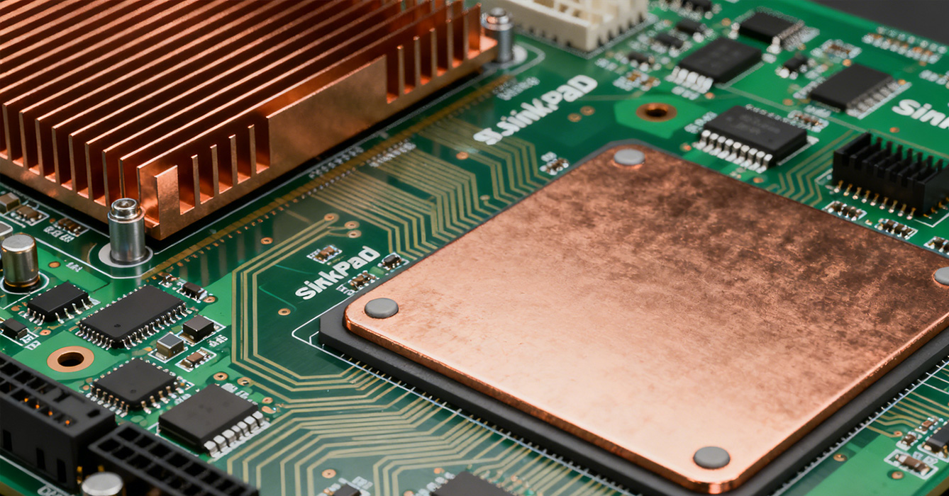
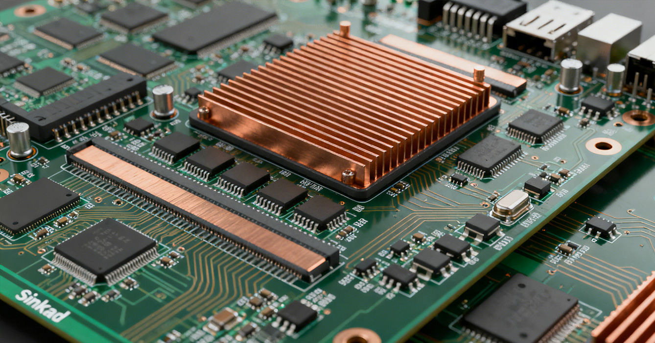
Sinkpad PCB has evolved from a niche thermal management component to a foundational technology enabling the next generation of high-power, compact electronic systems. As global demand for electrification, connectivity, and computational power accelerates, sinkpad PCBs have transcended traditional boundaries—adapting to diverse industries through material innovations, process refinements, and system-level integration. Unlike standard PCBs that prioritize signal routing alone, modern sinkpad PCBs harmonize thermal efficiency, mechanical robustness, and electrical performance, addressing the core pain points of power density growth in applications ranging from electric vehicles (EVs) to edge computing. This article explores the latest technical advancements, cross-industry integration strategies, emerging challenges, and future trajectories of sinkpad PCB technology, highlighting its role as a critical enabler of technological progress.
The performance leap of sinkpad PCBs is rooted in material science advancements that balance thermal conductivity, weight, and cost. While pure copper remains the gold standard for thermal transfer (401 W/(m·K)), next-generation sinkpad designs are embracing hybrid and composite materials to overcome limitations:
Nanocomposite Cores: Graphene-reinforced copper and carbon nanotube (CNT)-integrated aluminum cores offer 20-30% higher thermal conductivity than pure metals while reducing weight by 15-20%. These materials are particularly valuable for weight-sensitive applications like aerospace and wearable medical devices.
Ceramic-Metal Hybrids: Alumina (Al₂O₃) and aluminum nitride (AlN) ceramic substrates bonded with thin copper layers deliver exceptional thermal stability (operating temperatures up to 200°C) and dielectric strength, making them ideal for high-voltage industrial power electronics.
Sustainable Alternatives: Recycled copper cores (99.85% purity) and bio-based dielectrics are gaining traction, aligning with global sustainability goals without compromising performance. These eco-friendly materials reduce carbon footprints by 30-40% compared to conventional designs.
Manufacturing processes for sinkpad PCBs have undergone significant refinement to meet the demands of high-volume production and custom applications:
Laser Micro-Machining: High-precision laser drilling enables micro-scale thermal via arrays (diameter <0.1mm) with densities exceeding 20 vias/cm², enhancing heat dissipation without sacrificing board real estate. This process ensures uniform via placement, critical for dense component layouts in AI servers.
Low-Temperature Bonding: Advanced lamination techniques (e.g., plasma-activated bonding) enable the integration of dissimilar materials (e.g., copper and flexible polyimides) at temperatures <180°C, preventing thermal degradation and improving structural integrity. This innovation has unlocked the development of flexible sinkpad PCBs for conformal mounting in curved EV battery packs and wearable devices.
Additive Manufacturing: 3D-printed sinkpad structures, using conductive inks and thermal resins, offer unprecedented design flexibility—enabling complex geometries like internal micro-channels for liquid cooling. While still in early adoption, additive manufacturing reduces prototyping cycles by 50% and supports on-demand production of custom sinkpad configurations.
Modern sinkpad PCB design has shifted from component-level thermal management to system-level integration, leveraging simulation and AI-driven tools:
Thermal-Electrical Co-Simulation: Advanced software (e.g., ANSYS Icepak + HFSS) enables simultaneous optimization of thermal flow and signal integrity, eliminating trade-offs between heat dissipation and high-frequency performance. This is critical for 5G/6G RF modules, where thermal-induced signal loss can degrade connectivity.
AI-Powered Layout Design: Machine learning algorithms analyze thousands of design iterations to optimize sinkpad placement, via distribution, and copper pour patterns—reducing thermal resistance by 15-25% and cutting design time by 40%. These tools also predict reliability risks, such as thermal cycling-induced delamination, before production.
Modular Design: Standardized sinkpad modules (e.g., 10x10mm, 20x20mm) with interchangeable thermal interfaces enable rapid customization for diverse applications, from industrial motor drives to consumer electronics. This modularity reduces lead times and supports scalable production.

Sinkpad PCBs are tailored to address industry-specific challenges through targeted design and integration approaches:
EV Powertrains: Sinkpad PCBs with thick copper cores (4-6oz) and integrated thermal vias cool SiC MOSFETs and IGBTs in traction inverters, reducing junction temperatures by 30-40°C and extending battery range by 5-8%. Modular sinkpad designs support scalable powertrain configurations (from 100kW to 500kW).
Wireless Charging: Low-loss dielectric sinkpad PCBs with optimized ground planes minimize signal attenuation in 85kHz wireless charging systems, improving power transfer efficiency to >95%. Flexible sinkpad variants conform to underbody contours, enabling seamless integration in EVs.
Base Station Infrastructure: Sinkpad PCBs with copper-aluminum hybrid cores balance thermal management (cooling 50W RF amplifiers) and weight reduction, critical for tower-mounted 5G base stations. Low-loss dielectrics (e.g., Rogers 5880) maintain impedance stability across 3GHz-30GHz frequencies.
Edge Servers: Dense sinkpad arrays with liquid cooling micro-channels dissipate heat from high-performance CPUs/GPUs in edge computing modules, enabling 24/7 operation in space-constrained environments (e.g., factory floors, remote data centers).
Motor Drives: Ruggedized sinkpad PCBs with ceramic-copper hybrid cores withstand temperature cycling (-40°C to 125°C) and vibration in industrial motor drives, reducing downtime by 30%. Grid copper pour patterns enhance heat spreading in 24/7 operating conditions.
Solar Inverters: Sinkpad PCBs with corrosion-resistant finishes (e.g., ENEPIG) and UV-stable dielectrics handle high currents (200A+) in solar inverters, ensuring reliability in outdoor environments. Thermal vias connected to heat sinks reduce component temperatures by 25°C, extending lifespan to 25 years.
The integration of dissimilar materials (e.g., copper, ceramics, polymers) creates thermal expansion mismatches that can lead to delamination. Solutions include:
Stress-Relief Structures: Curved copper traces and dielectric buffer zones absorb thermal stress during temperature cycling.
CTE-Matched Materials: Newly developed dielectrics with CTE values (10-15 ppm/K) matching copper reduce interface stress by 40%.
As applications move to higher frequencies (e.g., 6G’s 100GHz+ bands), sinkpad PCBs face challenges with signal attenuation and EMI. Mitigation strategies:
Low-Loss Dielectrics: PTFE-based substrates and ceramic-filled polymers minimize dielectric loss (tanδ <0.002) at high frequencies.
Shielded Sinkpad Designs: Ground via arrays surrounding sinkpad regions confine electromagnetic energy, reducing EMI by 20-30%.
Advanced materials (e.g., diamond-copper composites) and processes (e.g., 3D printing) offer performance benefits but at higher costs. Addressing this:
Localized Material Optimization: Using premium materials only in critical thermal regions (e.g., sinkpad pedestals) while leveraging standard materials elsewhere reduces costs by 25-30%.
Automated Production Lines: Robotics and AI-driven inspection systems scale advanced manufacturing processes, lowering per-unit costs for high-volume applications (e.g., EVs).

Embedded Sensors: Miniature temperature and strain sensors integrated into sinkpad structures enable real-time monitoring of thermal and mechanical conditions, supporting predictive maintenance in critical applications (e.g., aerospace, medical devices).
Self-Healing Materials: Research into microcapsule-based self-healing dielectrics could extend sinkpad PCB lifespan by repairing small cracks caused by thermal cycling.
Space-Grade Sinkpads: Radiation-hardened materials and low-outgassing dielectrics will support sinkpad PCB use in satellite power systems and space exploration vehicles.
High-Temperature Applications: Silicon carbide (SiC) substrate-based sinkpads will operate reliably at 300°C+, targeting industrial process control and deep drilling equipment.
Circular Design: Thermoelectric separation structures will enable 95% material recovery from end-of-life sinkpad PCBs, supporting the circular economy.
Energy-Efficient Manufacturing: Solar-powered production lines and waterless etching processes will reduce the environmental impact of sinkpad PCB fabrication.
Sinkpad PCB technology has undergone a remarkable evolution, driven by the need for high-power, compact, and reliable electronic systems across industries. From material innovations like nanocomposite cores to AI-powered design optimization and cross-industry integration strategies, sinkpad PCBs continue to push the boundaries of thermal management and electrical performance. While challenges like thermal expansion mismatch and high-frequency signal integrity persist, ongoing research and development are unlocking solutions that will enable even more ambitious applications—from 6G infrastructure to humanoid robots. As a critical enabler of electrification, connectivity, and sustainability, sinkpad PCB technology will remain at the forefront of electronic innovation, shaping the future of high-power electronics for decades to come.

Got project ready to assembly? Contact us: info@apollopcb.com


We're not around but we still want to hear from you! Leave us a note:

Leave Message to APOLLOPCB
