


-
- PCB TYPE
- PRINTED CIRCUIT BOARD PROTOTYPE ALUMINUM PRINTED CIRCUIT BOARD R&F PCB FPC HIGH FREQUENCY PCB HIGH-TG PCB HEAVY COPPER PCB HDI PCB PCB FOR LIGHTING METAL CORE PCB

time:Nov 19. 2021, 09:29:33
In the electronics processing industry, it is the mantra of the industry. But what exactly is it? Now, Jingbang’s technicians will introduce you to the mysterious.
In fact, it is very simple, PCB is printed circuit board, that is, the abbreviation of Printed circuit board in English. It exists in every electronic device. A fully functional PCB is mainly used to create connections between components, such as resistors, capacitors, inductors, diodes, transistors, integrated chips, etc. It is the carrier of the entire logic circuit.
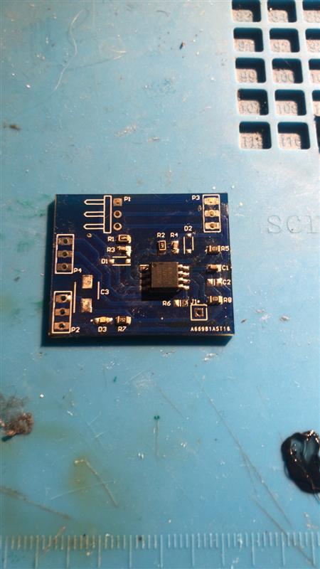
The bare board before mounting is often called "printed circuit board", or PWB for short. The PCB substrate is made of materials that are not easy to bend and are insulated and heat-insulated. The small lines visible to the naked eye on the surface of the PCB are conductive layers made of copper foil. First, the copper foil is covered on the entire PCB. Then the unnecessary copper foil part is etched with a special solution, then the remaining part becomes the tiny circuit we need. These copper foil lines are called wiring or wires, and their role is to connect the circuit between the parts on the PCB.
The color of common PCB boards is brown or green. This is the color of solder mask and the insulating layer of the PCB that plays a protective role. It can protect the copper wire and prevent the circuit from being affected by the wrong soldering of the components. A thin screen printing surface is usually printed on the solder mask. Symbols and text are usually printed on the screen printing surface, which can indicate the information and location of electronic components in a certain position. So the screen printing surface is also called the icon surface by us.

Got project ready to assembly? Contact us: info@apollopcb.com


 Whatsapp 0086 755 29438407
 Mail info@apollopcb.com
 Tel 0086 755 29438407


ABOUT US

PRODUCTS
TECHNOLOGY
KNOWLEDGE CENTRE
CULTURE
NEWS
We're not around but we still want to hear from you! Leave us a note:

Leave Message to APOLLOPCB
