-
- PCB TYPE
- PRINTED CIRCUIT BOARD PROTOTYPE ALUMINUM PRINTED CIRCUIT BOARD R&F PCB FPC HIGH FREQUENCY PCB HIGH-TG PCB HEAVY COPPER PCB HDI PCB PCB FOR LIGHTING METAL CORE PCB
In the world of electronics, aluminum PCBs (Printed Circuit Boards) are becoming an essential solution for many high-performance applications. Known for their excellent thermal conductivity and mechanical strength, aluminum PCBs are particularly effective in environments where heat dissipation is crucial. This article explores the advantages of aluminum PCBs, their key applications, and important considerations when selecting the right aluminum PCB for your electronic products.
An aluminum PCB is a type of metal core PCB that utilizes aluminum as the base material. This metal core allows for excellent heat management, making aluminum PCBs highly effective in applications where overheating is a concern. The structure of an aluminum PCB typically consists of three layers:
Copper Layer: This is the conductive layer where the circuit is etched.
Dielectric Layer: An insulating layer that is thermally conductive, allowing heat to pass through while electrically isolating the copper from the aluminum.
Aluminum Base Layer: This layer provides mechanical strength and excellent thermal conductivity, making it ideal for dissipating heat from components like LEDs, power devices, and other heat-sensitive electronics.
The ability of aluminum PCBs to efficiently conduct heat makes them an ideal choice for modern electronics.
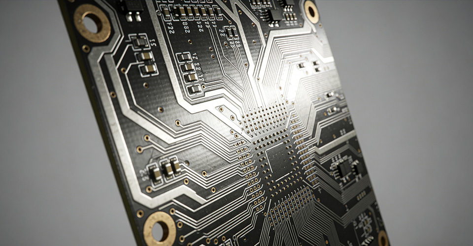
One of the most significant benefits of aluminum PCBs is their thermal conductivity. Aluminum’s natural ability to transfer heat helps keep components cool, ensuring that devices operate efficiently and last longer. In high-power applications, such as LED lighting and power electronics, managing heat is critical for preventing thermal damage and ensuring reliability.
The aluminum base provides mechanical strength to aluminum PCBs, making them more durable and capable of withstanding physical stresses. This is particularly useful in applications where the PCB may be subjected to vibration, impact, or other harsh conditions. Additionally, bendable aluminum PCBs offer flexibility, allowing them to be shaped and fitted into compact or irregular spaces without compromising their structural integrity.
Aluminum PCBs are often more cost-effective compared to copper-based PCBs, particularly when considering their thermal conductivity and mechanical properties. The relatively lower cost of aluminum makes it an attractive option for manufacturers looking to balance performance with cost.
With aluminum PCB’s efficient thermal conductivity, devices stay cooler and operate more reliably, which improves overall performance. This makes aluminum PCBs an ideal choice for industries such as automotive, telecommunications, and renewable energy, where device reliability and performance are paramount.
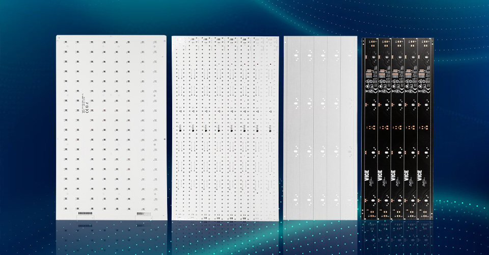
A Single Layer aluminum PCB consists of a single copper layer and is typically used in less complex applications. Single Layer aluminum PCBs are ideal for simpler designs, such as LED lighting modules, power supplies, and consumer electronics, where thermal management is needed but the design complexity is relatively low.
For more complex circuits requiring higher density, Multi-Layer aluminum PCBs are a better choice. These PCBs include multiple copper layers, which allow for more intricate circuit designs while still benefiting from the thermal conductivity of the aluminum base. Multi-Layer aluminum PCBs are commonly used in automotive control systems, high-performance power electronics, and advanced LED applications.
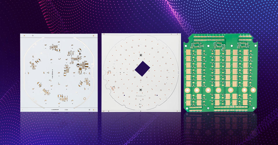
One of the most widespread applications of aluminum PCBs is in LED lighting. LEDs generate significant heat, and without proper heat management, their lifespan and performance can be compromised. Aluminum PCBs help dissipate the heat generated by LEDs, ensuring that they operate at optimal temperatures. Single Layer aluminum PCBs are typically used in smaller LED lighting applications, while Multi-Layer aluminum PCBs are used for more complex, high-power LED systems, such as those used in streetlights and automotive headlights.
In the automotive industry, aluminum PCBs are used for power control units, automotive lighting, sensors, and other critical electronics. Aluminum PCBs help ensure that automotive systems can operate reliably under the extreme conditions of temperature and vibration encountered in vehicles. The bendable aluminum PCB is particularly useful for automotive applications that require flexibility in design.
Aluminum PCBs are also used extensively in power electronics, where efficient heat dissipation is essential. These include power supplies, power converters, motor drives, and energy systems. By using aluminum PCBs, these high-power devices can operate more efficiently and with improved thermal stability, reducing the risk of component failure due to overheating.
In renewable energy systems, such as solar inverters and wind turbine controllers, aluminum PCBs are used to ensure that these high-power systems remain cool and operate optimally. The thermal conductivity of aluminum PCBs plays a critical role in maintaining the efficiency and reliability of renewable energy systems.
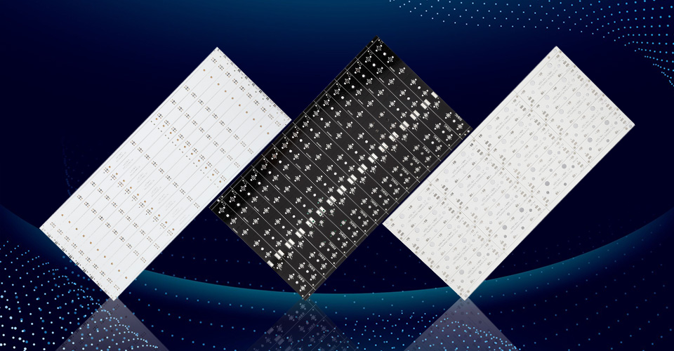
The thermal conductivity of aluminum PCBs is one of the key factors to consider when selecting the right PCB for your project. If the application involves high-power components that generate significant heat, opting for aluminum PCBs with a higher thermal conductivity is crucial for effective heat management.
If your design requires flexibility, bendable aluminum PCBs are an excellent option. These flexible boards allow for easy integration into compact or irregular spaces, making them ideal for applications such as wearable electronics and compact automotive components.
For less complex designs, a Single Layer aluminum PCB may be sufficient. However, if your circuit requires more layers and intricate routing, a Multi-Layer aluminum PCB will provide the necessary complexity and flexibility for high-density designs.
While aluminum PCBs are generally more affordable than copper-based PCBs, it is important to consider the specific thermal and mechanical needs of your application. The cost of Multi-Layer aluminum PCBs can be higher due to the increased complexity, so balancing performance requirements with budget constraints is essential.
Aluminum PCBs are a powerful solution for applications requiring effective thermal conductivity, durability, and reliability. From LED lighting to automotive electronics and power electronics, the advantages of aluminum PCBs are clear. Whether you need a Single Layer aluminum PCB for a basic design or a Multi-Layer aluminum PCB for a more complex system, aluminum-based PCBs offer exceptional performance and cost efficiency.
By understanding the key benefits, applications, and considerations of aluminum PCBs, you can make informed decisions to optimize your designs and improve the overall performance of your electronic devices.
Answer:
Single Layer aluminum PCBs are ideal for simple designs, offering excellent thermal conductivity and durability at a lower cost. They are commonly used in LED lighting and low-power electronics where basic heat management is needed.
Answer:
Multi-Layer aluminum PCBs incorporate multiple layers of copper for more complex circuits and higher density. They are used in advanced applications that require more intricate designs, such as automotive electronics and power supplies.
Answer:
Thermal conductivity in aluminum PCBs ensures that heat generated by components is effectively dissipated, preventing overheating and improving the longevity and reliability of the device. This is especially critical in high-power applications like power electronics and LED lighting.
Answer:
Bendable aluminum PCBs are flexible boards that allow for customization in design, making them ideal for applications with space constraints or unique form factors, such as wearable electronics and automotive systems.
Answer:
Aluminum-based PCBs are generally more affordable than copper-based PCBs and offer excellent thermal conductivity for heat-sensitive applications. Copper-based PCBs are preferred for applications requiring superior thermal and electrical performance, but aluminum PCBs provide a more cost-effective solution for many designs.
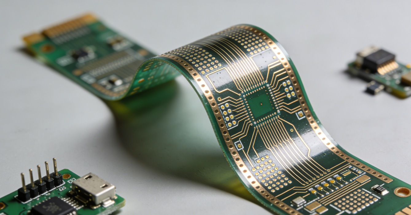
In the dynamic world of electronics, the need for components that balance performance, adaptability, and compactness has never been greater. Flexible printed circuit boards (Flex PCBs) have emerged as a transformative solution, redefining how devices are designed and built across industries. At the center of this innovation stands the flexible PCB manufacturer— a key partner that turns conceptual designs into functional, reliable components capable of powering everything from everyday gadgets to cutting-edge industrial systems. As technology evolves, the role of a trusted flexible PCB manufacturer becomes increasingly critical, bridging the gap between design ambition and real-world application.
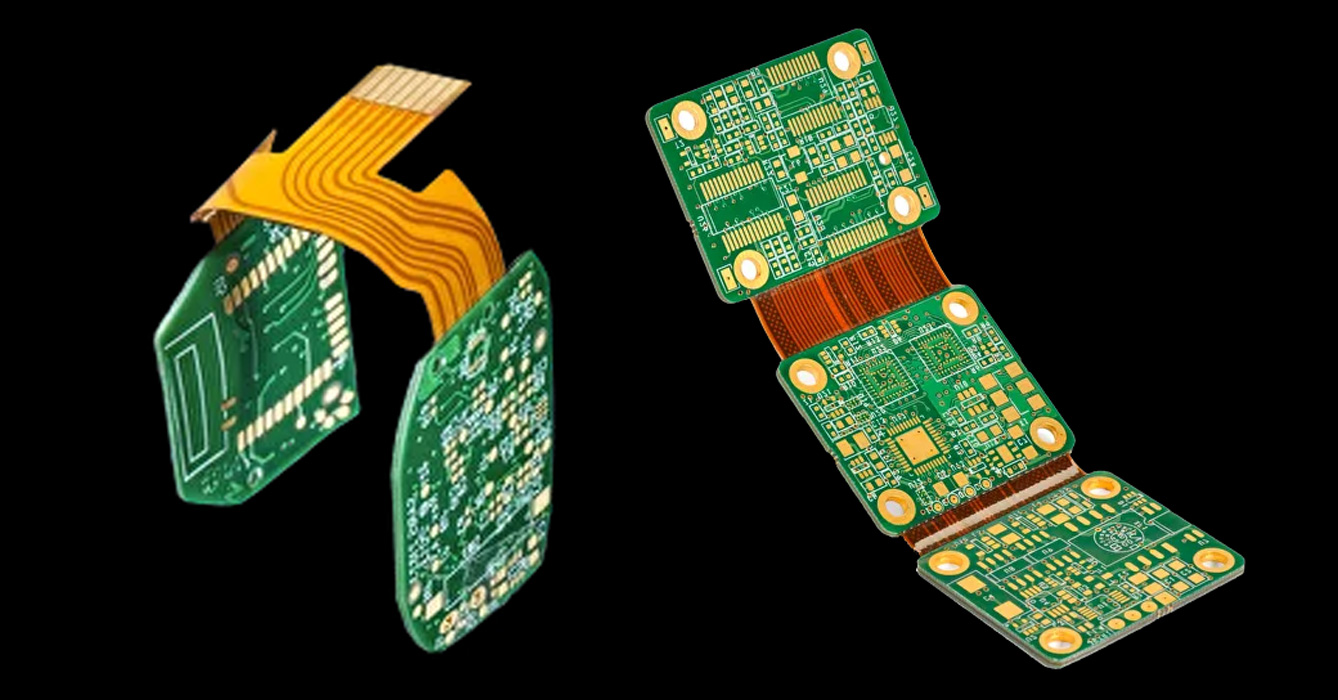
Flex PCBs differ from traditional rigid circuit boards by offering unmatched flexibility, bendability, and lightweight properties. This unique combination allows them to fit into tight spaces, conform to irregular shapes, and withstand dynamic environments—qualities that are non-negotiable in modern device design. However, harnessing these benefits requires specialized expertise that only a dedicated flexible PCB manufacturer can provide. Unlike generic circuit board producers, these manufacturers focus exclusively on mastering the nuances of flexible materials and production processes, ensuring that each board delivers consistent performance regardless of its application. From wearable fitness trackers that curve with the body to industrial sensors that operate in high-vibration settings, a skilled flexible PCB manufacturer tailors solutions to meet the unique demands of each use case.
A top-tier flexible PCB manufacturer does not limit its expertise to a single industry—instead, it adapts its capabilities to serve a wide range of sectors, each with distinct needs. In the consumer electronics space, these manufacturers enable the sleek, foldable designs of smartphones and laptops, as well as the miniaturization of wireless earbuds and smart home devices. The automotive industry relies on flexible PCB manufacturers to produce components for advanced driver-assistance systems (ADAS), infotainment setups, and electric vehicle (EV) powertrains, where durability and space efficiency are paramount. In healthcare, flexible PCBs power life-saving devices like portable diagnostic tools and wearable health monitors, where biocompatibility and precision are critical. Even in aerospace and defense, flexible PCB manufacturers deliver components that withstand extreme temperatures and harsh conditions, supporting satellite systems and military equipment. Across all these sectors, the ability to adapt and innovate makes the flexible PCB manufacturer an indispensable partner for progress.
Not all flexible PCB manufacturers are created equal—several core attributes set industry leaders apart. First and foremost is a commitment to quality. Reputable manufacturers implement rigorous quality control processes at every stage of production, from material selection to final testing, ensuring that each flexible PCB meets international standards and client specifications. They also invest in advanced technology and skilled engineering teams, enabling them to tackle complex designs and stay ahead of emerging trends. Flexibility in production is another key trait: leading manufacturers can accommodate both small-batch prototypes and large-scale production runs, adapting to the unique needs of startups and established enterprises alike. Additionally, exceptional customer collaboration is a hallmark of a trusted flexible PCB manufacturer. They work closely with clients to understand their goals, offer technical guidance, and refine designs to optimize performance and manufacturability—turning challenges into opportunities for innovation.
As technology continues to advance, the flexible PCB manufacturer is poised to play an even more pivotal role in driving innovation. The rise of the Internet of Things (IoT) is increasing demand for compact, low-power flexible PCBs that can connect billions of smart devices. The growth of wearable technology and augmented reality (AR) devices requires even greater flexibility and miniaturization, pushing manufacturers to develop thinner, more durable boards. Additionally, the shift toward sustainable manufacturing is prompting flexible PCB manufacturers to adopt eco-friendly materials and processes, aligning with global efforts to reduce environmental impact. By staying ahead of these trends, investing in research and development, and prioritizing customer needs, the flexible PCB manufacturer is not just adapting to change—they are leading it.
In a world where electronic devices are becoming more specialized, compact, and versatile, the flexible PCB manufacturer remains a cornerstone of innovation. By combining technical expertise, quality craftsmanship, and cross-industry adaptability, these manufacturers empower businesses to bring groundbreaking products to market. Whether you’re developing a consumer gadget, a medical device, or an industrial system, partnering with the right flexible PCB manufacturer is the key to unlocking the full potential of your design. As technology evolves, the value of a trusted flexible PCB manufacturer will only grow—proving that versatility, reliability, and collaboration are the foundation of success in the modern electronics landscape.
In the era of rapid technological innovation, electronic devices are becoming increasingly specialized—demanding components that adapt to unique designs, environments, and functional requirements. Flexible printed circuit boards (Flex PCBs) have emerged as a cornerstone of this evolution, offering versatility, compactness, and durability that rigid PCBs cannot match. For businesses seeking to turn their unique concepts into reality, partnering with a reputable Custom Flexible PCB Manufacturer is a strategic choice that bridges design ambition with practical functionality. These specialized manufacturers prioritize customization, crafting Flex PCBs tailored to the specific needs of industries ranging from consumer tech to medical devices and beyond.
Generic, off-the-shelf Flex PCBs may serve basic purposes, but they often fail to meet the nuanced demands of modern electronic design. Every device has distinct spatial constraints, performance goals, and environmental conditions—whether it’s a wearable health monitor requiring ultra-thin flexibility, an industrial sensor needing resistance to extreme temperatures, or a aerospace component demanding lightweight reliability. A Custom Flexible PCB Manufacturer addresses these gaps by working closely with clients to develop solutions that align with their exact specifications. Unlike mass-produced alternatives, custom Flex PCBs eliminate unnecessary features, optimize form factors, and integrate design elements that enhance overall device performance, making them indispensable for innovative products.
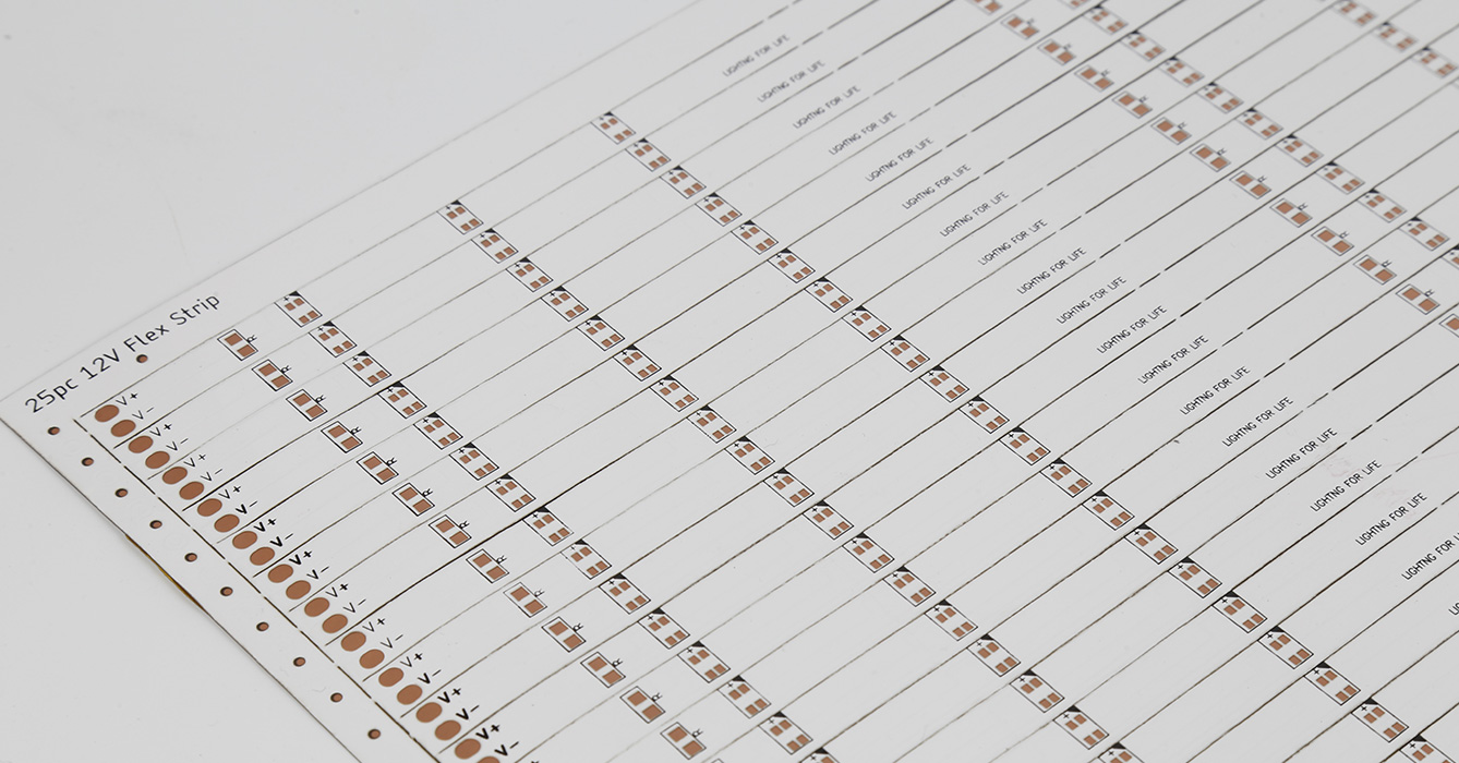
A top-tier Custom Flexible PCB Manufacturer excels at adapting to the unique needs of diverse sectors, proving that customization is not a one-size-fits-all process but a tailored approach to each industry’s challenges. In consumer electronics, custom Flex PCBs enable the sleek, foldable designs of smartphones and tablets, as well as the compactness of wireless earbuds and smartwatches. The medical industry relies on custom solutions for devices like implantable monitors and portable diagnostic tools, where biocompatibility, miniaturization, and precise signal transmission are non-negotiable. Automotive manufacturers turn to Custom Flexible PCB Manufacturers for components that fit into tight engine bays or curved interior panels, supporting advanced driver-assistance systems (ADAS) and electric vehicle technology. Even in industrial settings, custom Flex PCBs withstand harsh conditions, powering sensors and control systems that operate in dusty, high-vibration environments. Across all these fields, the ability to customize ensures that Flex PCBs do not just fit into devices—they elevate their capabilities.
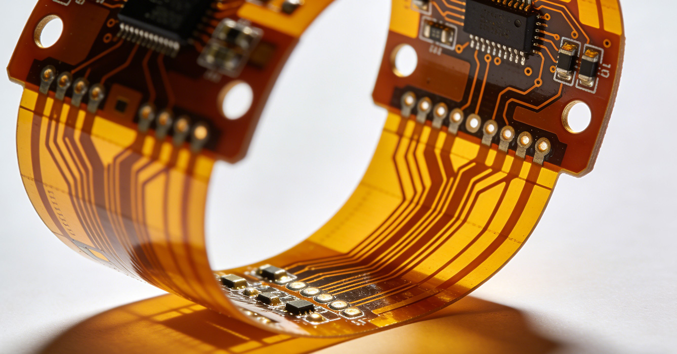
The success of a custom Flex PCB project hinges on collaboration between the manufacturer and the client. A trusted Custom Flexible PCB Manufacturer does more than execute designs; they act as technical partners, bringing expertise to every stage of the process. From the initial consultation, their engineering teams work to understand the client’s goals, address design challenges, and offer insights to optimize performance and manufacturability. Whether it’s suggesting material modifications to improve flexibility, adjusting layouts to reduce signal interference, or refining designs to meet regulatory standards, this collaborative approach ensures that the final product not only meets expectations but exceeds them. Prototyping is a key part of this journey, allowing clients to test and refine custom Flex PCBs before full-scale production, minimizing risks and ensuring alignment with their vision.
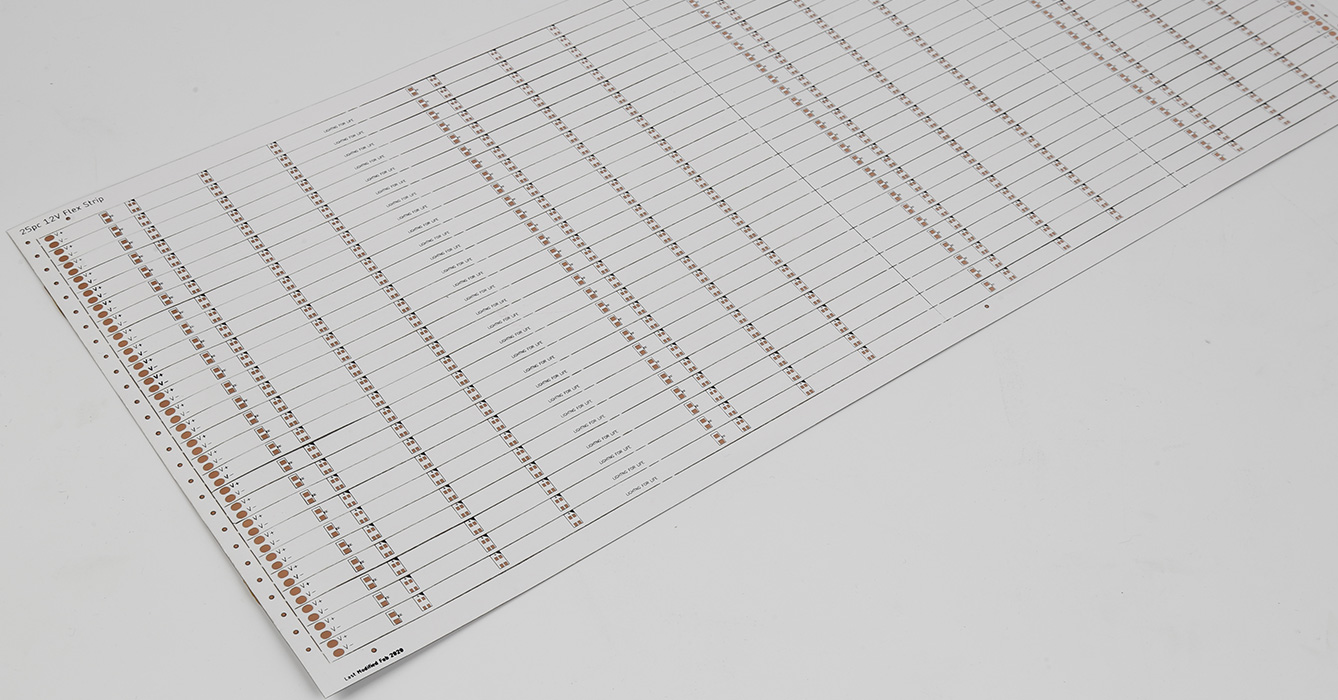
Not all Custom Flexible PCB Manufacturers are created equal—several key traits distinguish the industry leaders. First and foremost is a commitment to quality: reputable manufacturers implement rigorous quality control measures throughout the customization and production process, ensuring that each custom Flex PCB adheres to international standards and client specifications. They also invest in advanced technology and skilled engineering teams, enabling them to tackle complex designs and stay ahead of industry trends. Flexibility in production is another critical factor, as leading manufacturers can accommodate both small-batch prototypes and larger production runs without compromising on customization or lead times. Finally, exceptional customer support—from initial design discussions to post-delivery assistance—fosters long-term partnerships, as clients trust that their unique needs will be prioritized at every step.
As electronic devices continue to evolve in complexity and specialization, the demand for tailored solutions will only grow. A Custom Flexible PCB Manufacturer plays a pivotal role in this ecosystem, turning innovative ideas into functional, reliable components that drive progress across industries. By prioritizing customization, collaboration, and quality, these manufacturers empower businesses to differentiate their products, overcome design challenges, and succeed in a competitive global market. Whether you’re developing a groundbreaking wearable device, a life-saving medical tool, or a next-generation automotive component, partnering with the right Custom Flexible PCB Manufacturer is the key to unlocking the full potential of your design—proving that when it comes to electronic components, one size never fits all.
In today’s fast-paced electronic landscape, the demand for flexible printed circuit boards (Flex PCBs) continues to surge—driven by the need for compact, lightweight, and durable components in devices ranging from consumer electronics to industrial machinery. For businesses scaling their production lines, partnering with a reliable High Volume Flex PCB Manufacturer is no longer an option but a strategic necessity. These specialized manufacturers play a pivotal role in translating innovative designs into mass-produced, high-quality Flex PCBs that meet the rigorous standards of global industries.
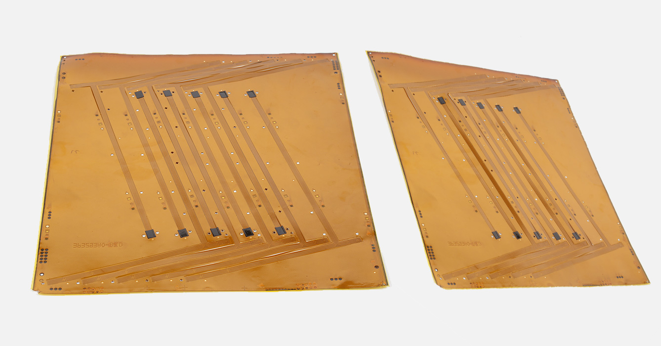
The rise of smart devices, wearable technology, automotive electronics, and medical equipment has amplified the need for Flex PCBs that can keep up with high-volume production without compromising performance. Unlike traditional rigid PCBs, Flex PCBs offer unparalleled flexibility, allowing them to fit into tight spaces and adapt to complex device geometries. However, producing these boards in large quantities requires specialized expertise, advanced manufacturing processes, and a commitment to consistency—all hallmarks of a top-tier High Volume Flex PCB Manufacturer.
One of the key reasons businesses prioritize partnering with a dedicated High Volume Flex PCB Manufacturer is the ability to achieve economies of scale. These manufacturers leverage state-of-the-art production facilities, automated assembly lines, and optimized supply chains to produce Flex PCBs in bulk at competitive costs. By streamlining processes from design validation to final assembly, they eliminate inefficiencies that often plague small-scale production, ensuring timely delivery even for the most demanding order volumes. This scalability is critical for businesses looking to meet market demand, expand their customer base, or launch new products on a global scale.
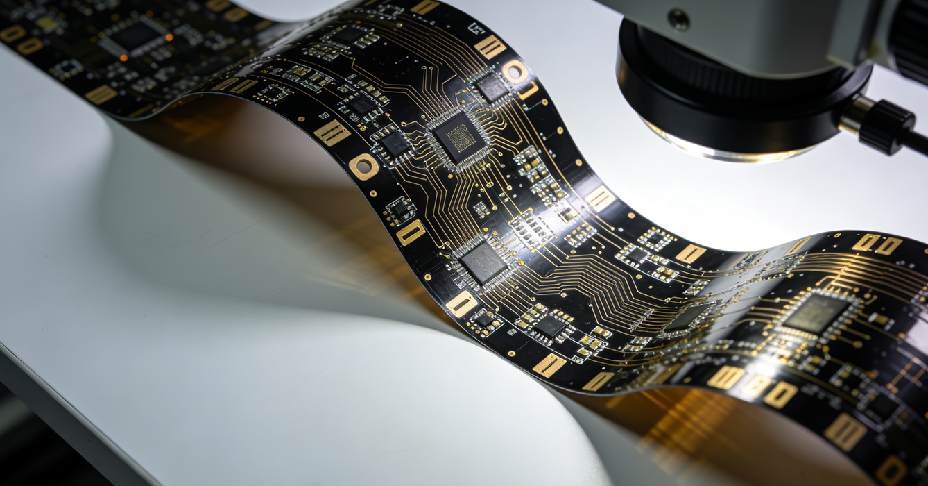
Quality control is another non-negotiable aspect of high-volume Flex PCB production. A reputable High Volume Flex PCB Manufacturer implements rigorous testing protocols at every stage of the manufacturing process. From material inspection to electrical performance testing, each batch of Flex PCBs undergoes strict quality checks to ensure compliance with international standards. This attention to detail minimizes the risk of defects, reduces downtime for customers, and upholds the reliability of end products. For industries like healthcare and automotive, where product failure can have serious consequences, partnering with a manufacturer that prioritizes quality is essential.
Beyond production capacity and quality, a leading High Volume Flex PCB Manufacturer offers valuable technical support and collaboration. These manufacturers work closely with clients to optimize designs for high-volume production, providing insights on material selection, layout efficiency, and cost-saving opportunities. Their engineering teams have the expertise to address complex design challenges, ensuring that Flex PCBs not only meet technical specifications but also align with production timelines and budget constraints. This collaborative approach fosters long-term partnerships, as clients benefit from a trusted advisor who understands their unique needs and industry requirements.
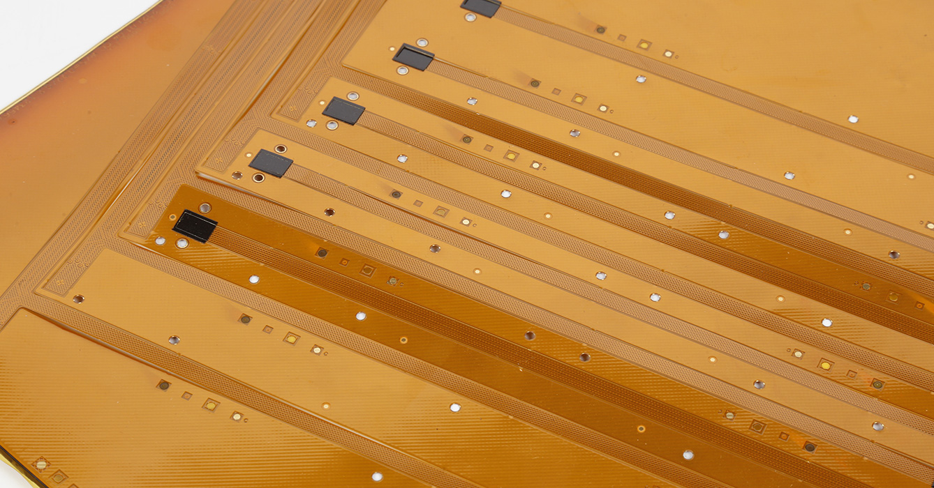
The applications of high-volume Flex PCBs are vast and diverse. In the consumer electronics sector, they power smartphones, tablets, and wearable devices, enabling sleek designs and reliable performance. In automotive manufacturing, Flex PCBs are used in advanced driver-assistance systems (ADAS), infotainment systems, and electric vehicle components, where durability and space efficiency are paramount. The medical industry relies on high-volume Flex PCBs for diagnostic equipment, wearable health monitors, and implantable devices, where precision and biocompatibility are critical. Across all these sectors, a High Volume Flex PCB Manufacturer serves as the backbone of innovation, enabling businesses to bring cutting-edge products to market efficiently.
In a global market defined by rapid technological advancements and increasing competition, choosing the right High Volume Flex PCB Manufacturer can give businesses a significant edge. These manufacturers combine scalability, quality, and technical expertise to deliver Flex PCBs that meet the demands of high-volume production while supporting innovation. Whether a business is launching a new product line, expanding into new markets, or seeking to optimize its supply chain, partnering with a specialized High Volume Flex PCB Manufacturer is a strategic investment that pays dividends in reliability, cost savings, and market success.
As the demand for flexible electronics continues to grow, the role of High Volume Flex PCB Manufacturers will only become more critical. By staying ahead of industry trends, investing in advanced technology, and prioritizing customer collaboration, these manufacturers are poised to drive the next wave of innovation in high-scale electronic production. For businesses looking to thrive in a dynamic market, aligning with a trusted High Volume Flex PCB Manufacturer is the key to unlocking scalability, quality, and long-term growth.
Sinkpad PCB has evolved into a universal core component for high-power electronic systems, transcending niche application boundaries to become a linchpin of modern electrification and digitalization. Unlike standard PCBs that prioritize signal routing, sinkpad technology integrates specialized thermal management structures with robust electrical performance, addressing the critical challenge of concentrated heat dissipation in power-dense devices. From NEVs and industrial automation to consumer electronics and medical equipment, sinkpad PCBs enable the miniaturization, efficiency, and reliability of next-generation electronics. This article explores the latest global technological innovations, cross-industry application expansions, market dynamics, and future trajectories of sinkpad PCB, highlighting its role as a catalyst for technological advancement across sectors.
| Feature | Standard MCPCB | Apollo Sinkpad PCB | Performance Impact |
| Thermal Path | Through Dielectric Layer | Direct-to-Metal Contact | Zero thermal resistance at the dielectric |
| Conductivity | 1.0 - 4.0 W/m·K | Up to 400 W/m·K (Copper) | Dramatic temperature drop for high-power chips |
| Structure | Circuit - Dielectric - Base | Direct Solder Pad on Base | Prevents thermal throttling in LEDs |
| Ideal Power | 1W - 5W per LED | 10W - 100W+ per LED | Essential for automotive & industrial UV |
| Reliability | Moderate (Dielectric aging) | Extreme (Metal bonding) | Significantly extends product service life |
Global manufacturers and research institutions are pushing the boundaries of sinkpad PCB materials to balance thermal conductivity, weight, durability, and cost:
Nanomaterial-Reinforced Composites: Graphene-infused copper and carbon nanotube (CNT)-aluminum hybrids have emerged as game-changers, offering 30-40% higher thermal conductivity than pure metals while reducing weight by 20-25%. These materials are increasingly adopted in aerospace and portable high-power devices, where weight efficiency is paramount.
Ceramic-Metal Matrix Composites (CMMCs): Aluminum nitride (AlN) and silicon carbide (SiC) ceramic cores bonded with thin copper layers deliver exceptional thermal stability (operating temperatures up to 300°C) and dielectric strength, making them ideal for high-voltage industrial power electronics and electric vehicle powertrains.
Flexible Thermal Substrates: Polyimide-copper laminates with enhanced thermal conductivity (>200 W/(m·K)) enable conformal sinkpad PCBs, adapting to curved surfaces in wearable devices, automotive battery packs, and flexible industrial sensors.
Innovative structural designs are unlocking new levels of thermal and electrical performance:
3D-Printed Micro-Cooling Channels: Additive manufacturing technologies enable the integration of micro-scale liquid or air cooling channels directly within sinkpad cores, reducing thermal resistance by 40-50% compared to traditional passive designs. This innovation is critical for ultra-high-power applications like AI server GPUs and industrial inverters.
Hierarchical Thermal Paths: Multi-layered sinkpad structures with gradient copper thickness—thicker layers near heat sources, thinner layers for signal routing—optimize heat dissipation while maximizing routing density. This design balances thermal efficiency with space constraints in compact devices like smartphone fast-charging modules.
Integrated EMI Shielding: Sinkpad cores are engineered with built-in electromagnetic interference (EMI) shielding layers, eliminating the need for separate shielding components and reducing system complexity. This is particularly valuable for RF and high-frequency applications like 5G base station power amplifiers.
Industry 4.0 technologies are transforming sinkpad PCB production, enhancing precision, scalability, and reliability:
AI-Driven Process Optimization: Machine learning algorithms analyze real-time production data (e.g., lamination temperature, drilling speed, etching depth) to predict defects and adjust parameters dynamically, reducing scrap rates by 15-20% and improving batch-to-batch consistency.
Digital Twin Simulation: Virtual replicas of sinkpad PCB designs and production lines enable pre-production testing of thermal performance, mechanical stress, and electrical integrity, cutting development cycles by 30-35%.
Automated Inspection Technologies: High-resolution X-ray CT, ultrasonic testing, and AI-powered optical inspection (AOI) systems ensure 100% detection of internal defects (e.g., voids, delamination) and surface irregularities, meeting the strict quality requirements of critical applications like medical devices and aerospace electronics.
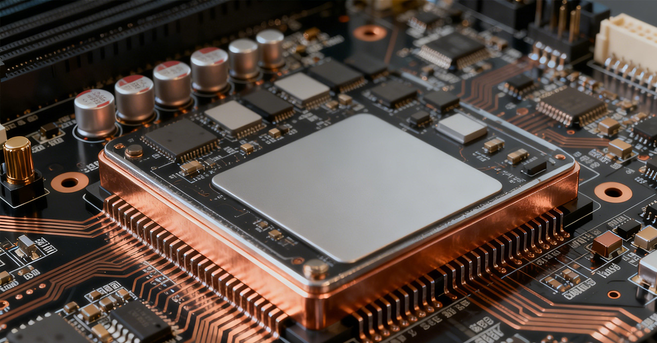
Sinkpad PCB’s versatility has driven its adoption across diverse high-power electronic sectors, each with tailored requirements:
On-Board Chargers (OBCs): Sinkpad PCBs with copper-aluminum hybrid cores handle high currents (200-400A) in fast-charging systems, reducing charging time while maintaining thermal stability.
Battery Management Systems (BMS): Conformal sinkpad PCBs monitor and balance battery cell temperatures, preventing thermal runaway and extending battery lifespan.
Electric Powertrains: Ceramic-copper sinkpad PCBs cool SiC and GaN power semiconductors in traction inverters, withstanding extreme temperatures (-40°C to 150°C) and vibration.
Industrial Inverters & Converters: Sinkpad PCBs with integrated cooling channels manage heat from high-power IGBTs and diodes in 100kW+ industrial systems, ensuring 24/7 operation with minimal downtime.
Motor Drives: Low-profile sinkpad designs enable compact motor drive units, reducing footprint while cooling high-current motor controllers in robotics and manufacturing equipment.
High-Power Charging Adapters: Sinkpad PCBs with thin-gauge copper cores (2-3oz) enable 65W+ fast chargers with slim form factors, dissipating heat efficiently without overheating.
Gaming Consoles & PCs: Copper-core sinkpad PCBs cool high-performance CPUs and GPUs, preventing thermal throttling and enhancing gaming performance.
Medical Imaging Equipment: Sinkpad PCBs with radiation-resistant materials cool high-power X-ray and MRI components, ensuring precise imaging while complying with medical safety standards.
Aerospace Power Systems: Lightweight, high-strength sinkpad PCBs with ceramic-copper cores power avionics and satellite systems, withstanding extreme temperature fluctuations and radiation in space.
Electrification of Transportation: The global shift toward EVs is a primary driver, with NEV production expected to reach 54 million units by 2030, boosting demand for automotive-grade sinkpad PCBs.
Industrial Automation & Robotics: The adoption of Industry 4.0 technologies is increasing the need for high-power, compact industrial electronics, driving sinkpad PCB growth in manufacturing sectors.
5G & 6G Infrastructure Deployment: The expansion of high-speed mobile networks requires power-dense base stations and repeaters, creating significant demand for low-loss, thermally efficient sinkpad PCBs.
Asia-Pacific Dominance: China, South Korea, and Japan lead the global sinkpad PCB market, accounting for 65-70% of production. Chinese manufacturers leverage complete industrial chains and cost advantages, while South Korean and Japanese firms focus on high-end, specialized applications (e.g., aerospace, medical).
North American & European Growth: Regional manufacturers are expanding production capacity to meet demand from EV makers and industrial automation firms, with a focus on sustainable and high-performance solutions.
Emerging Markets: Southeast Asia and India are emerging as manufacturing hubs, attracting investments from global electronics firms due to lower labor costs and growing local demand.
Eco-Friendly Materials: The use of recycled copper (99.85% purity) and bio-based dielectrics is increasing, reducing carbon footprints by 30-40% compared to traditional manufacturing.
Circular Manufacturing: Thermoelectric separation designs enable efficient material recovery from end-of-life sinkpad PCBs, supporting circular economy goals and reducing electronic waste.
Energy-Efficient Production: Solar-powered factories, waterless etching processes, and energy-saving equipment are becoming standard, aligning with global sustainability regulations (e.g., EU Green Deal, China’s "Dual Carbon" goals).
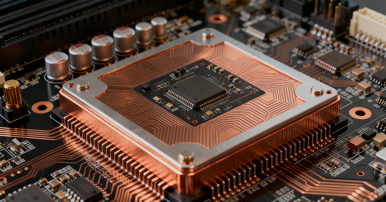
2D Material Integration: Transition metal dichalcogenides (TMDs) and MXenes are being explored for sinkpad cores, offering thermal conductivity exceeding 1000 W/(m·K) and enabling ultra-compact, high-power designs.
Self-Healing Polymers: Research into self-healing dielectric materials could extend sinkpad PCB lifespan by repairing micro-cracks caused by thermal cycling and mechanical stress.
Embedded Sensors & IoT Connectivity: Sinkpad PCBs will integrate temperature, strain, and humidity sensors with IoT connectivity, enabling real-time monitoring and predictive maintenance in critical applications.
Adaptive Thermal Management: Smart sinkpads with adjustable cooling channels or phase-change materials will dynamically respond to thermal loads, optimizing energy efficiency and performance.
Space-Grade Sinkpads: Radiation-hardened materials and low-outgassing dielectrics will support sinkpad PCB use in deep-space exploration and satellite systems.
High-Temperature Industrial Applications: Silicon carbide (SiC) and diamond-copper composite sinkpads will operate reliably at 400°C+, targeting industrial process control and geothermal energy systems.
Sinkpad PCB has evolved from a specialized thermal management component to a universal enabler of high-power, compact electronic systems across industries. Driven by global innovations in materials, structural design, and manufacturing, sinkpad PCBs are addressing the core challenges of electrification, digitalization, and sustainability. From EV powertrains and industrial automation to consumer electronics and aerospace, their versatility and performance make them indispensable for next-generation technologies. As the demand for higher power density, smaller form factors, and greener solutions continues to grow, sinkpad PCB technology will remain at the forefront of electronic innovation—shaping a more efficient, connected, and sustainable future. The global market’s focus on cross-domain integration, smart manufacturing, and sustainable practices will drive further advancements, solidifying sinkpad PCB’s role as a critical component in the electronics ecosystem.
[Contact ApolloPCB Today for a Free Review and Precision Quote]
Related Articles:
Sinkpad PCB: Zero-Dielectric-Resistance Thermal Management | ApolloPCB
LED Lighting Sinkpad PCB stands as a foundational component in modern illumination systems, addressing the unique thermal and mechanical demands of LED technology. Unlike generic PCBs, this specialized solution is engineered to manage the concentrated heat generated by LED chips— a critical factor that directly impacts lumen maintenance, energy efficiency, and lifespan. As LED lighting evolves toward higher power densities, smaller form factors, and diverse applications (from residential downlights to industrial high-bays), LED Lighting Sinkpad PCB has become indispensable for unlocking the full potential of energy-efficient illumination. This article explores the illumination-specific design considerations, material optimizations, application-driven innovations, and performance validation of LED Lighting Sinkpad PCB, highlighting its role in shaping reliable, sustainable lighting solutions.
LED Lighting Sinkpad PCB design is tailored to the unique operating characteristics of LED systems, balancing thermal efficiency with form factor and application requirements.
LEDs convert only 20-30% of energy into light, with the rest dissipated as heat—concentrated in a small chip area. LED Lighting Sinkpad PCB addresses this by optimizing thermal paths for illumination scenarios:
Direct Chip-to-Sinkpad Contact: For high-power LEDs (30W+), the sinkpad’s metal core is precision-aligned with the LED’s thermal pad, eliminating intermediate layers to minimize thermal resistance. This direct path ensures heat is rapidly transferred away from the junction, preventing lumen depreciation.
Size-Scaled Heat Spreading: Compact fixtures (e.g., residential bulbs) use slim, disc-shaped sinkpads that match the LED’s footprint, while high-bay lights employ extended sinkpad structures with radial heat channels to cover larger areas. This scaling ensures thermal efficiency without compromising fixture design.
Passive Cooling Synergy: Sinkpad geometries are integrated with fixture housings to leverage natural convection—critical for lighting applications where active cooling (fans) is impractical due to noise or size constraints.
LED Lighting Sinkpad PCB is designed to adapt to the diverse form factors of modern lighting:
Low-Profile Designs: For slim fixtures like panel lights and track lights, sinkpad PCBs use thin-gauge metal cores (1-2mm) with optimized copper pour patterns, maintaining thermal performance while enabling sleek aesthetics.
Conformal Compatibility: Flexible sinkpad PCBs (using polyimide substrates) conform to curved surfaces, supporting innovative designs such as automotive headlight strips and architectural contour lighting.
Component Integration: Sinkpad layers are engineered to accommodate LED drivers, resistors, and connectors in a single board, reducing fixture complexity and assembly costs—key for mass-produced lighting products.
LED Lighting Sinkpad PCB must withstand the specific environmental stresses of lighting applications:
Outdoor Lighting: Sinkpad cores and finishes (e.g., anodized aluminum, ENEPIG plating) resist UV radiation, moisture, and temperature cycling (-40°C to 65°C), ensuring long-term performance in street lights and floodlights.
Indoor Commercial Spaces: Humidity-resistant dielectrics and corrosion-proof traces address the stable but high-usage environments of offices, retail stores, and hospitals, where lighting operates 12+ hours daily.
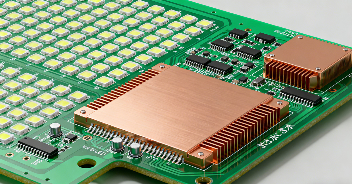
Materials and manufacturing processes for LED Lighting Sinkpad PCB are optimized to balance performance, cost, and scalability—critical for the competitive lighting market.
Aluminum Core Dominance: For mid-to-high-power LED lighting (10-50W), aluminum-core sinkpads offer a cost-effective balance of thermal conductivity (237 W/(m·K)) and weight, making them ideal for mass-produced fixtures like downlights and street lights.
Copper Core for High-Power Needs: High-bay lights and industrial lighting (50W+) use copper-core sinkpads to handle higher thermal loads, leveraging copper’s superior conductivity (401 W/(m·K)) to maintain lower junction temperatures.
Hybrid Composites for Specialized Use: Ceramic-aluminum hybrids are used in extreme-temperature applications (e.g., industrial process lighting), combining thermal stability with dielectric strength to withstand 150°C+ operating conditions.
Precision Etching for Fine Traces: LED Lighting Sinkpad PCB requires narrow electrical traces (0.2-0.5mm) to fit compact fixtures, using controlled etching processes to maintain trace integrity while preserving the sinkpad’s thermal path.
Solder Mask Optimization: Clear solder mask is applied to sinkpad surfaces (except LED mounting areas) to enhance heat dissipation and protect against environmental damage, without interfering with thermal transfer.
Scalable Production: Manufacturers use automated assembly lines for LED Lighting Sinkpad PCB, ensuring consistent quality for high-volume lighting applications—critical for meeting the demands of residential and commercial construction projects.
LED Lighting Sinkpad PCB must meet strict illumination-specific standards to ensure reliability and energy efficiency.
Lumen Maintenance Validation: Sinkpad performance is tested alongside LEDs per IES LM-80 standards, tracking lumen output over 6,000+ hours to ensure ≥90% retention—directly linking thermal management to lighting performance.
Thermal Cyclic Testing: Simulates seasonal temperature changes for outdoor lighting, subjecting sinkpad PCBs to 500+ cycles of -40°C to 85°C to verify structural integrity and thermal consistency.
Energy Efficiency Benchmarking: Tests per ENERGY STAR requirements measure lumens per watt (lm/W) with the sinkpad installed, ensuring the design contributes to the fixture’s energy-saving claims.
IES LM-80: Mandates thermal management requirements for LED modules, ensuring sinkpad PCBs maintain junction temperatures within safe limits to preserve lifespan.
ENERGY STAR: Requires LED fixtures with sinkpad PCBs to achieve minimum lm/W ratios (e.g., ≥80 lm/W for residential bulbs), validating energy efficiency.
RoHS/REACH: Restricts hazardous substances in sinkpad materials, aligning with global lighting industry sustainability mandates and enabling market access in Europe and North America.
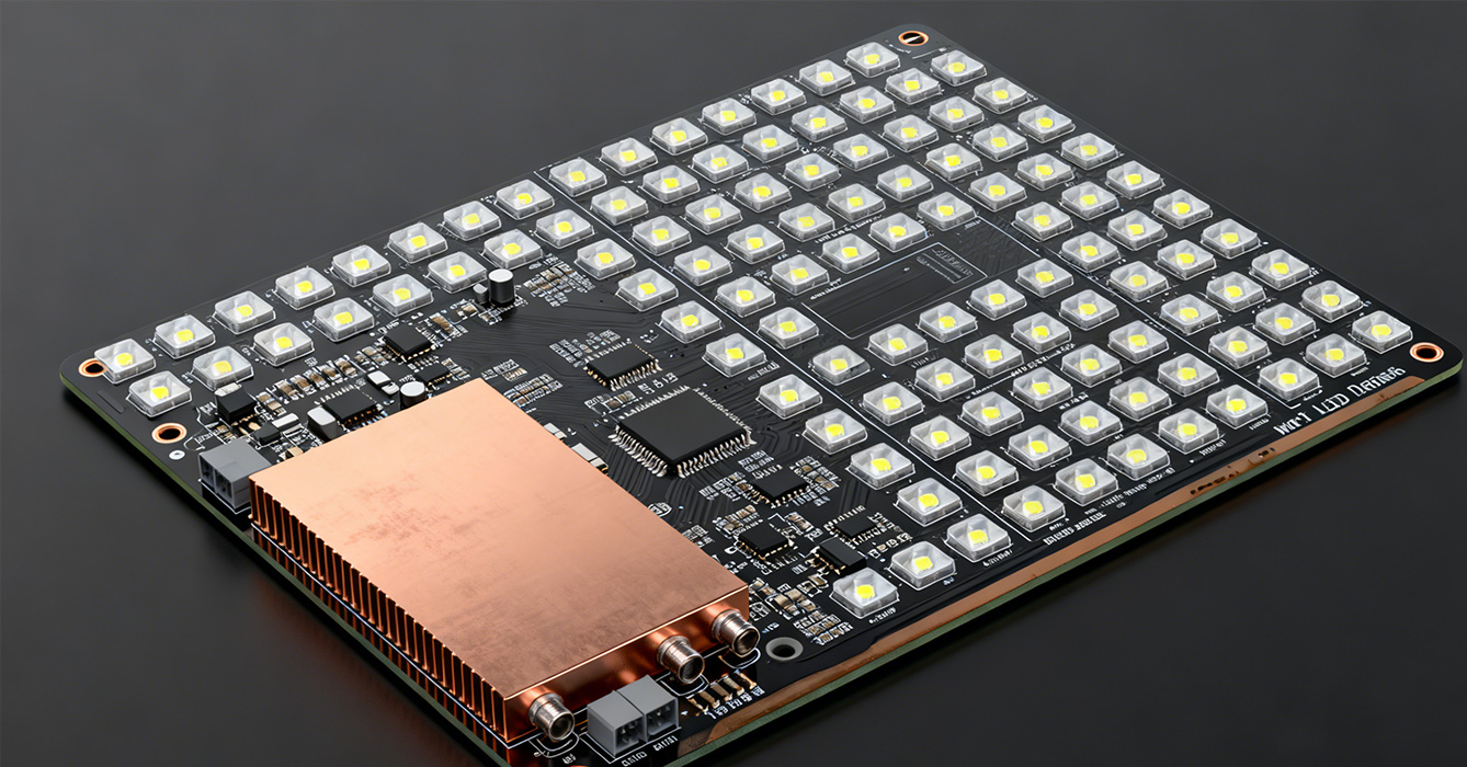
High-Bay Lights: Copper-core sinkpad PCBs dissipate heat from 100W+ LEDs in warehouses and factories, maintaining 50,000+ hours of operation with minimal lumen loss.
Retail Track Lights: Low-profile aluminum sinkpads enable slim designs while cooling 30-50W LEDs, preserving color consistency (Δu'v' ≤0.005) critical for product displays.
Street Lights: Corrosion-resistant sinkpad PCBs with extended heat spreading structures handle 50-200W LEDs, enduring rain, UV, and temperature fluctuations for 100,000+ hours.
Landscape Lighting: Flexible sinkpad PCBs conform to curved fixtures, cooling 10-30W LEDs while withstanding moisture and soil contact.
LED Bulbs: Compact aluminum sinkpads fit within standard bulb envelopes, cooling 5-20W LEDs to extend lifespan beyond 25,000 hours.
Smart Downlights: Sinkpad PCBs integrate with wireless modules and dimming circuits, balancing thermal management with electrical integration for connected home systems.
Integrated Sensing: Sinkpad PCBs will embed low-power temperature sensors to enable adaptive dimming, adjusting LED output based on thermal conditions to maximize efficiency.
Eco-Friendly Materials: Recycled aluminum cores and bio-based dielectrics will become standard, reducing the carbon footprint of LED lighting systems.
Miniaturized High-Power Designs: Advanced thermal engineering will enable smaller sinkpad PCBs for high-power LEDs, supporting ultra-compact fixtures for urban and architectural applications.
LED Lighting Sinkpad PCB is a specialized, application-driven technology that unlocks the reliability and efficiency of modern LED illumination. By tailoring thermal paths, materials, and form factors to the unique needs of lighting systems—from compact residential bulbs to industrial high-bays—this solution addresses the core challenge of heat management in LEDs. Compliance with illumination-specific standards ensures performance consistency, while scalable manufacturing supports mass-market accessibility. As LED lighting continues to dominate the global illumination market, LED Lighting Sinkpad PCB will remain a critical enabler, driving innovations in energy efficiency, design flexibility, and sustainability for a brighter, greener future.
Energy-saving LED sinkpad design has become a critical focal point in the push for sustainable lighting, as it directly impacts both operational efficiency and environmental footprint. While LEDs inherently consume less power than traditional lighting technologies, their energy-saving potential is often untapped due to inadequate thermal management. Suboptimal sinkpad designs can lead to increased energy use, shortened lifespans, and compromised performance—undermining the sustainability goals of lighting systems. Unlike generic thermal solutions, energy-saving LED sinkpads require a holistic engineering approach that balances heat dissipation, material efficiency, and compliance with global energy standards. This article addresses the key engineering challenges, rigorous validation methods, industry compliance frameworks, and real-world implementation insights for energy-saving LED sinkpad design, providing a practical guide for engineers and manufacturers.
Developing effective energy-saving LED sinkpads requires overcoming interconnected challenges that span thermal, mechanical, and material engineering.
The primary challenge lies in integrating thermal management with electrical efficiency and mechanical practicality. LEDs operate most efficiently within a narrow thermal range, but sinkpad designs must also accommodate electrical traces, mounting constraints, and environmental stressors. For example, reducing sinkpad thickness to minimize material use can compromise thermal conductivity, while adding cooling features may increase weight and installation complexity. Engineers must navigate these trade-offs to create designs where thermal dissipation enhances energy efficiency without sacrificing structural integrity or electrical performance. This synergy is particularly critical in compact fixtures, where space limitations amplify the impact of every design decision.
Energy-saving LED sinkpads must perform reliably across diverse environmental conditions, from extreme temperatures in outdoor lighting to humidity in commercial spaces. Temperature fluctuations cause thermal expansion and contraction, which can degrade material bonds and create air gaps—increasing thermal resistance and forcing LEDs to consume more power to maintain brightness. For outdoor applications, sinkpads must resist corrosion, UV radiation, and moisture, as these factors reduce thermal efficiency over time. Balancing environmental durability with energy-saving goals requires selecting materials and finishes that withstand harsh conditions without adding unnecessary thermal mass or reducing heat transfer capabilities.
While advanced materials and designs can enhance energy savings, they often come with higher upfront costs. Engineers face the challenge of developing sinkpads that deliver long-term energy efficiency gains without pricing themselves out of the market. This requires prioritizing cost-effective materials (e.g., recycled aluminum over copper-graphene composites for mid-range applications) and optimizing designs to reduce manufacturing complexity. The goal is to create a total cost of ownership advantage, where lower energy bills offset any initial cost premium over standard sinkpads.
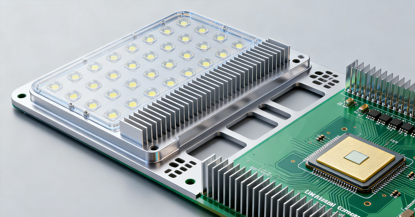
Ensuring the performance of energy-saving LED sinkpads requires specialized validation methods that measure both thermal efficiency and energy consumption.
Thermal Performance Testing
Infrared (IR) Thermography: Captures real-time temperature distribution across the sinkpad and LED junction, identifying hotspots that indicate inefficient heat transfer. This non-destructive test verifies that the sinkpad maintains uniform temperatures, a key factor in reducing energy use.
Thermal Resistance Measurement: Uses laser flash analysis (LFA) to quantify thermal resistance (Rθ) between the LED junction and sinkpad surface. Lower thermal resistance directly translates to reduced energy consumption, as LEDs operate at cooler temperatures.
Thermal Cycling Testing: Subjects sinkpads to repeated temperature cycles (-40°C to 85°C) to simulate real-world conditions, ensuring thermal efficiency remains consistent over time. This test validates that material bonds and thermal paths do not degrade, preserving energy-saving performance for the sinkpad’s lifespan.
Power Consumption Profiling: Measures LED driver power draw under different thermal conditions, comparing energy use with standard sinkpad designs. Validates that the energy-saving sinkpad reduces power consumption by 5-20% as intended, without compromising lumen output.
Lumen Maintenance Tracking: Monitors lumen output over 10,000+ hours to ensure energy savings do not come at the cost of performance. Energy-saving sinkpads should maintain ≥90% lumen output, as reduced brightness would force users to increase power to compensate.
Life-Cycle Energy Analysis: Calculates total energy use across the sinkpad’s lifespan, including manufacturing, transportation, operation, and disposal. This holistic analysis verifies that energy savings during operation outweigh any embodied energy from production.
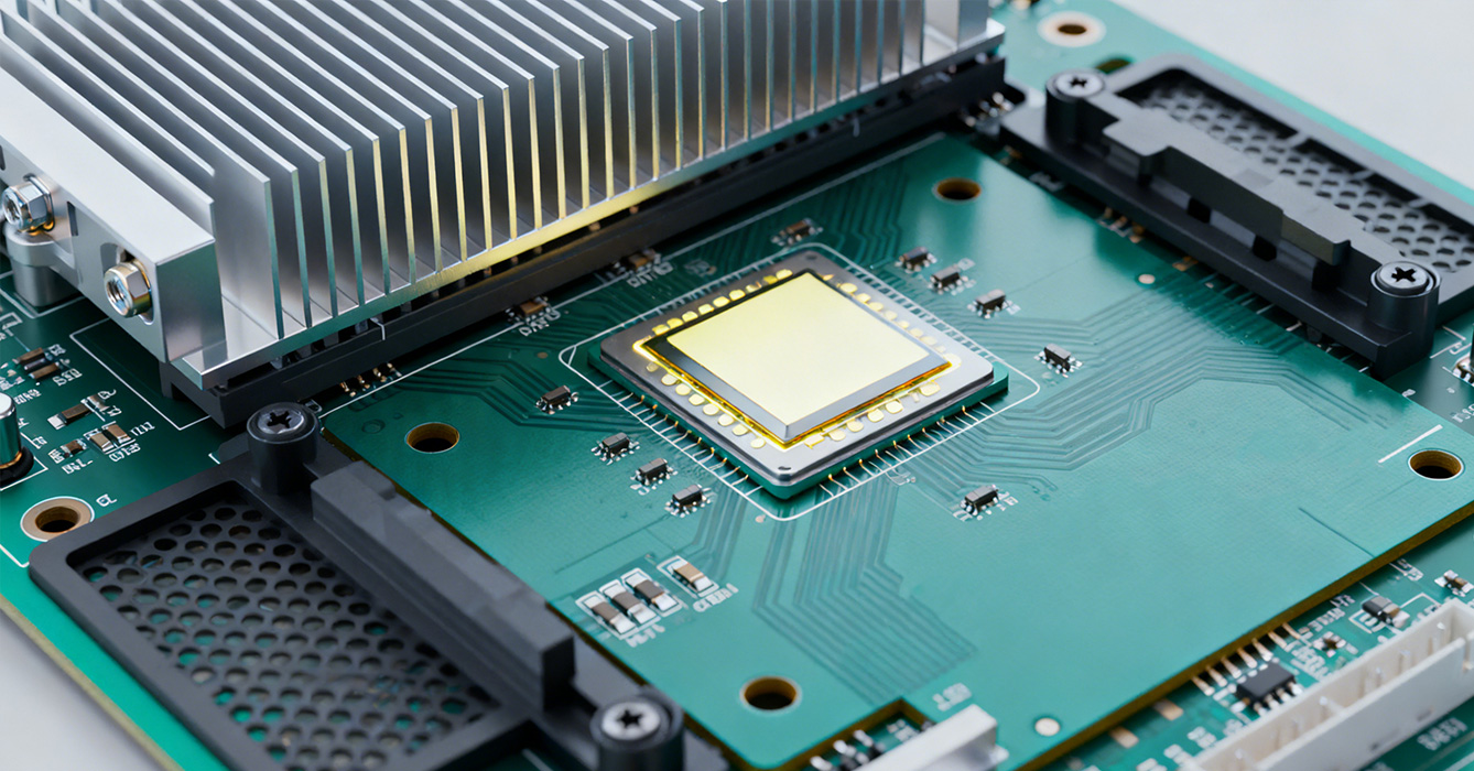
Energy-saving LED sinkpad designs must align with global standards and certifications to validate their efficiency claims and ensure market acceptance.
ENERGY STAR: Requires LED lighting systems to meet strict energy efficiency criteria, with sinkpad design playing a key role in achieving the required lumens per watt (lm/W) ratio. ENERGY STAR-certified fixtures with optimized sinkpads typically consume 75% less energy than incandescent lights.
IES LM-80: Specifies performance requirements for LED packages, modules, and arrays, including thermal management expectations. Sinkpad designs must support LM-80 compliance by maintaining junction temperatures within specified limits, ensuring consistent lumen output and energy efficiency.
EU ErP Directive: Mandates minimum energy performance standards for lighting products sold in the European Union. Energy-saving sinkpads help manufacturers meet ErP’s lm/W requirements and reduce the environmental impact of their products.
RoHS/REACH Compliance: Restricts hazardous substances in sinkpad materials, ensuring environmental safety during manufacturing and disposal. Using recycled metals and eco-friendly finishes helps meet these requirements while reducing carbon footprint.
BREEAM/LEED Integration: Supports green building certifications by contributing to energy efficiency and sustainability goals. Lighting systems with energy-saving sinkpads can earn points toward BREEAM or LEED certification, making them attractive for commercial and residential projects.
In smart office buildings, energy-saving LED sinkpads are integrated with occupancy sensors and natural light harvesting systems. For example, a 10-story office tower in Chicago used aluminum-fin sinkpads with low-loss thermal interfaces, reducing lighting energy consumption by 22% compared to standard designs. The sinkpads’ passive cooling eliminated fan energy use, while integration with smart controls adjusted power based on occupancy and ambient light—delivering annual energy savings of 30,000 kWh.
Solar street lights in rural areas rely on energy-saving sinkpads to maximize battery life. A project in Spain used corrosion-resistant sinkpads with integrated micro-channels, reducing LED power demand by 18%. This extended the lights’ runtime by 2.5 hours per night during low-sunlight months, eliminating the need for grid backup and reducing carbon emissions by 1.2 tons annually per 100 lights.
Energy-saving LED sinkpad design is a complex engineering endeavor that requires balancing thermal efficiency, environmental adaptability, and cost-effectiveness. By addressing core challenges such as thermal-electrical-mechanical synergy and environmental durability, engineers can create designs that unlock the full energy-saving potential of LED lighting. Rigorous validation methods—from thermal resistance testing to life-cycle energy analysis—ensure these designs perform as intended, while compliance with global standards like ENERGY STAR and ErP validates their efficiency claims. Real-world implementations in smart buildings and solar lighting demonstrate that energy-saving sinkpads deliver tangible benefits, reducing energy consumption, lowering costs, and supporting sustainability goals. As the lighting industry continues to prioritize efficiency and environmental responsibility, energy-saving LED sinkpad design will remain a critical technology, driving innovation and enabling a greener future.
In the world of electronics, precision is key. High precision IC substrate PCBs (Printed Circuit Boards) are at the heart of modern electronic devices, enabling faster processing speeds, smaller form factors, and increased functionality. These components are indispensable in the development of advanced electronics, impacting everything from smartphones to complex computing systems. In this article, we will delve into the intricacies of high precision IC substrate PCBs, their manufacturing process, and their importance in the electronics industry.
IC (Integrated Circuit) substrate PCBs serve as the foundation for the assembly of ICs. They provide the necessary interconnections between the ICs and other components within an electronic device. High precision PCBs are specifically engineered to meet stringent requirements for accuracy and reliability, making them suitable for high-performance applications.
Miniaturization: With the trend towards smaller and more powerful devices, high precision PCBs are designed to support miniaturization. This involves creating complex circuitry in a compact space without compromising on performance.
High Density Interconnect (HDI): These PCBs utilize HDI technology to increase the number of connections per unit area. This allows for more components to be integrated into a smaller footprint.
Enhanced Thermal Management: Proper heat dissipation is crucial for maintaining the performance and longevity of electronic devices. High precision PCBs incorporate materials and designs that improve thermal management.
High Frequency Performance: These PCBs are optimized for high-frequency applications, ensuring minimal signal loss and interference.
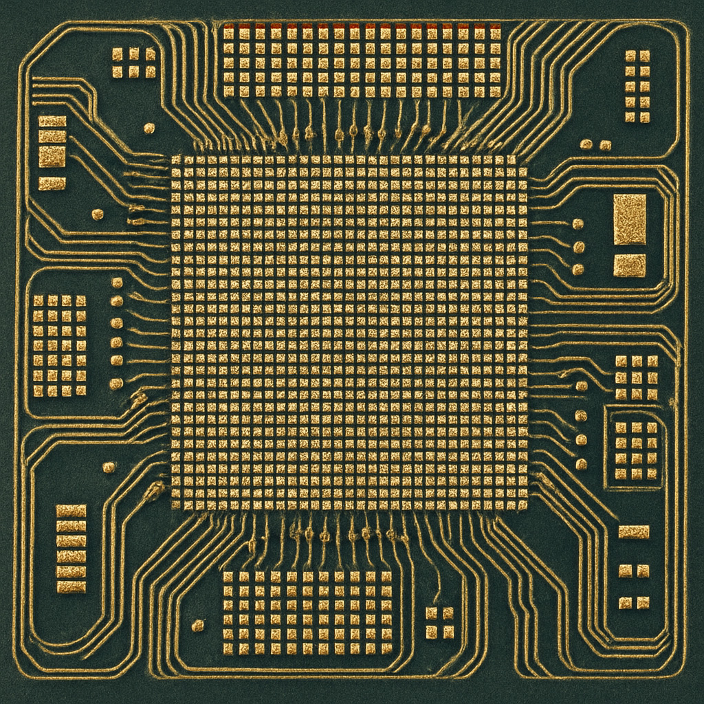
Creating high precision IC substrate PCBs requires a meticulous manufacturing process that involves several steps to ensure quality and performance.
The process begins with the design and layout of the PCB. Engineers use computer-aided design (CAD) software to create detailed schematics of the circuit. This stage involves specifying the placement of components, routing of traces, and defining layer stack-ups.
Choosing the right materials is crucial for achieving the desired electrical and thermal properties. Common materials include FR-4 (a glass-reinforced epoxy laminate) and advanced substrates like BT (Bismaleimide Triazine) resin and polyimide.
Photolithography is used to transfer the circuit pattern onto the substrate. A photosensitive film, known as a photoresist, is applied to the substrate. The PCB is then exposed to ultraviolet light through a mask that defines the circuit pattern. This process creates a hardened image of the circuit on the substrate.
The next step is etching, where unwanted copper is removed from the substrate to reveal the circuit pattern. Chemicals such as ferric chloride or ammonium persulfate are used to dissolve the excess copper.
Drilling is performed to create holes for component leads and vias (connections between layers). These holes are then plated with copper to ensure electrical connectivity.
A solder mask is applied to the PCB to protect the traces from oxidation and prevent solder bridges during component assembly. The solder mask also enhances the board's durability and electrical insulation.
The surface finish is applied to the exposed copper areas to protect them from oxidation and ensure good solderability. Common finishes include HASL (Hot Air Solder Leveling), ENIG (Electroless Nickel Immersion Gold), and OSP (Organic Solderability Preservative).
Rigorous testing is conducted to ensure that the PCB meets the required specifications. This includes electrical testing to verify connectivity and functional testing to assess performance under simulated conditions.
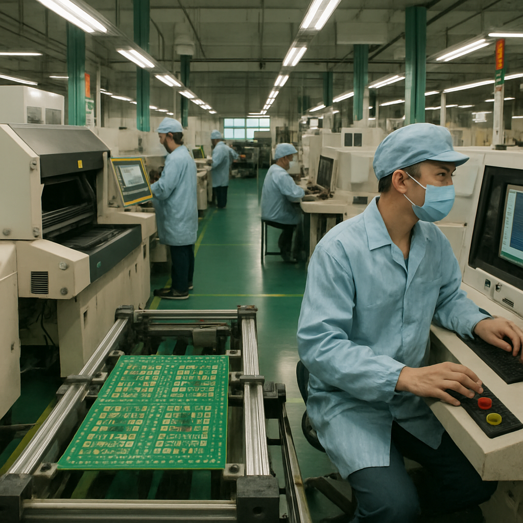
High precision IC substrate PCBs play a critical role in the advancement of technology. Their precision and reliability are crucial for the functionality of high-performance electronic devices. Here are some of the key benefits:
Increased Performance: High precision PCBs support faster data processing speeds and improved signal integrity, which are essential for modern electronic devices.
Space Efficiency: The ability to integrate more components into a smaller space allows for the development of compact and lightweight devices.
Enhanced Reliability: These PCBs are designed to withstand harsh environmental conditions, ensuring consistent performance over time.
Cost-Effectiveness: While the initial manufacturing cost may be higher, the durability and performance of high precision PCBs can lead to cost savings in the long run due to reduced failures and maintenance.
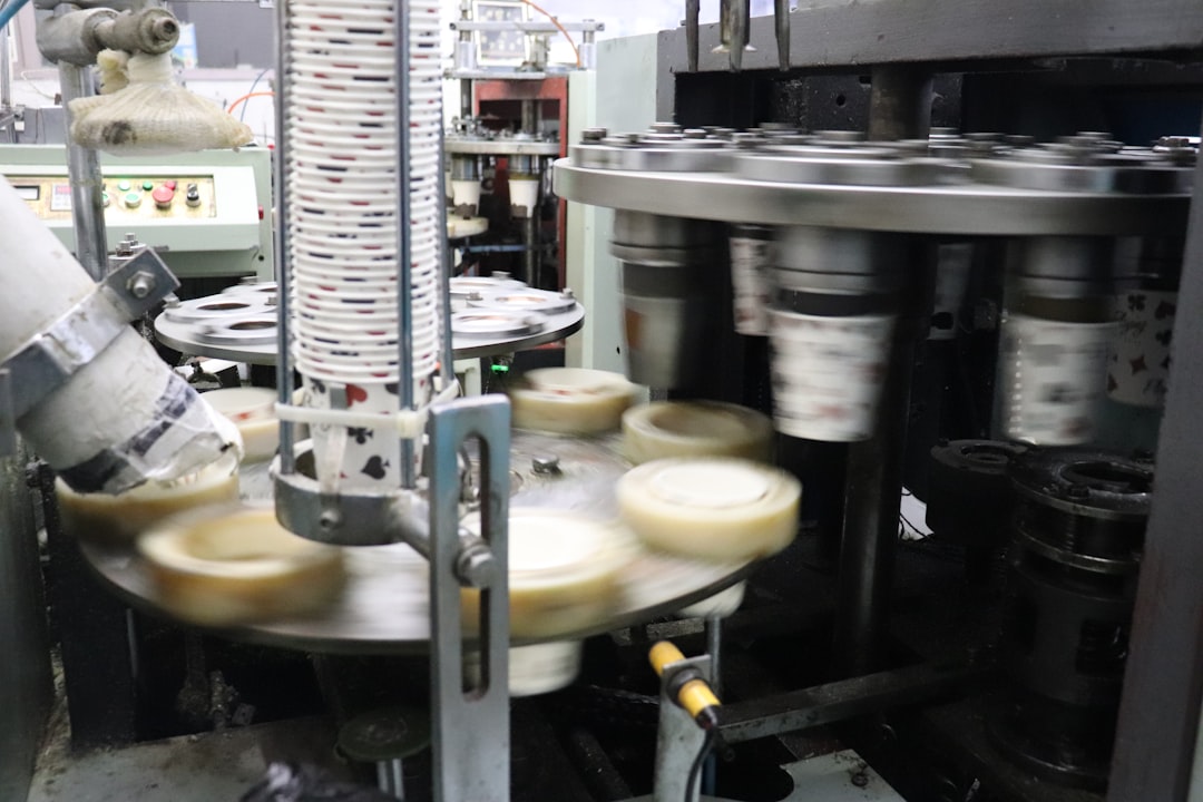
High precision PCBs are used in a variety of applications across different industries. Some of these include:
Consumer Electronics: Smartphones, tablets, and wearables rely on high precision PCBs for their compact designs and advanced functionalities.
Automotive Industry: Modern vehicles incorporate sophisticated electronic systems for navigation, entertainment, and safety, all of which depend on high precision PCBs.
Telecommunications: High-frequency communication devices require PCBs that can handle high data rates with minimal interference.
Medical Devices: Precision and reliability are paramount in medical equipment, making high precision PCBs essential for diagnostic and monitoring devices.
High precision IC substrate PCBs are indispensable components in the world of electronics. Their ability to support miniaturization, enhance performance, and improve reliability makes them vital for the development of advanced electronic devices. As technology continues to evolve, the demand for high precision PCBs will only increase, driving innovations in the manufacturing process and expanding their applications across various industries.
By understanding the intricacies of high precision IC substrate PCBs and their manufacturing process, businesses and engineers can make informed decisions that contribute to the success of their electronic products.
Thermal Conductive CEM3 PCB Material represents a strategic evolution of traditional Composite Epoxy Material-3 (CEM3), addressing one of the key limitations of standard CEM3: moderate thermal conductivity. By integrating thermal enhancement technologies into the classic CEM3 structure—retaining its non-woven glass core, woven glass outer layers, and epoxy matrix—this advanced material offers improved heat dissipation while preserving the cost-effectiveness and mechanical stability that make CEM3 a staple in electronics. Designed for applications where heat accumulation can compromise performance (but extreme thermal resistance is unnecessary), thermal conductive CEM3 bridges the gap between standard CEM3 and high-cost, high-thermal materials like metal-core PCBs (MCPCBs) or ceramic substrates. This article explores the composition, performance advantages, manufacturing innovations, and target applications of thermal conductive CEM3 PCB material, highlighting its role in enabling reliable operation in heat-sensitive devices.
Standard CEM3 excels in electrical insulation, mechanical stability, and flame resistance, but its epoxy matrix and glass fiber reinforcement inherently limit thermal conductivity. This can be a drawback in devices where even moderate heat generation—from components like small power transistors, LED drivers, or motor controllers—can lead to:
Performance Degradation: Elevated temperatures can reduce the efficiency of semiconductors, causing signal delays or voltage fluctuations in circuits.
Reduced Lifespan: Thermal cycling (repeated heating and cooling) can weaken solder joints and cause delamination, shortening PCB lifespan.
Safety Risks: In enclosed devices, heat buildup may exceed safety thresholds, even if the material meets flame resistance standards.
Thermal Conductive CEM3 PCB Material addresses these issues by improving heat transfer from hot components to the PCB edges or heat sinks, maintaining operating temperatures within safe limits without sacrificing CEM3’s core advantages.
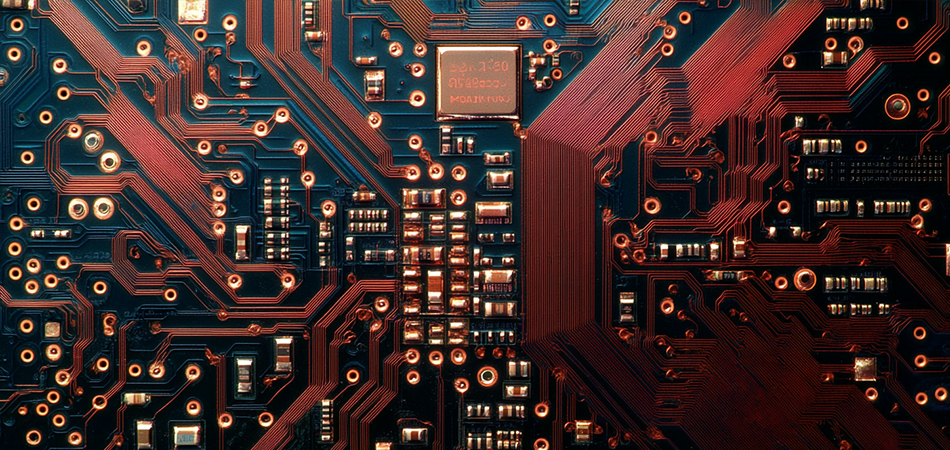
Thermal conductive CEM3 retains the hybrid structure of traditional CEM3 but incorporates targeted modifications to enhance heat dissipation:
The epoxy resin—historically a thermal insulator—is modified with thermally conductive fillers, such as:
Ceramic Particles: Aluminum oxide (Al₂O₃) or boron nitride (BN) particles, which improve thermal conductivity while maintaining electrical insulation. These fillers create a “thermal pathway” through the resin, allowing heat to flow more efficiently.
Graphene or Carbon Nanotubes: In small concentrations, these nanomaterials enhance thermal conductivity without compromising the resin’s adhesion to glass fibers or copper.
The filler concentration is carefully balanced: too little, and thermal performance gains are minimal; too much, and the resin may lose flexibility or adhesion, undermining mechanical stability.
While glass fibers themselves are not highly thermally conductive, their orientation and density in thermal conductive CEM3 are adjusted to:
Reduce Thermal Barriers: Ensuring the non-woven core and woven outer layers are free of voids, which can trap heat.
Align with Heat Flow Paths: Woven fabric layers are slightly adjusted to minimize resistance to heat moving from the PCB’s center (where components are mounted) to its edges.
Thicker copper foil (or copper with a textured surface) is sometimes used to improve heat spreading. Copper, a highly conductive material, distributes heat from hot components across the PCB surface, reducing hotspots. This complements the enhanced epoxy matrix, creating a synergistic effect in heat management.
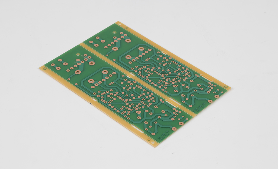
Thermal conductive CEM3 retains the practical advantages of standard CEM3 while delivering meaningful improvements in heat dissipation:
While not matching the conductivity of MCPCBs or ceramics, thermal conductive CEM3 typically offers 2–3 times better thermal conductivity than standard CEM3. This is sufficient to reduce operating temperatures by 10–20°C in devices with moderate heat generation—enough to prevent performance issues in applications like LED light fixtures or small motor controllers.
Mechanical Stability: The material retains sufficient flexural strength and dimensional stability to support standard components, resisting warping even under thermal stress.
Electrical Insulation: Thermally conductive fillers are chosen for their electrical insulating properties, ensuring dielectric strength and insulation resistance remain comparable to standard CEM3. This is critical for preventing short circuits in high-density designs.
Flame Resistance: Modifications preserve UL94 V-0 certification, ensuring safety in enclosed devices like consumer electronics or industrial control panels.
Thermal conductive CEM3 costs 10–20% more than standard CEM3 but remains 30–50% cheaper than MCPCBs or ceramic substrates. This makes it an economical choice for applications where heat management is important but extreme performance is unnecessary.
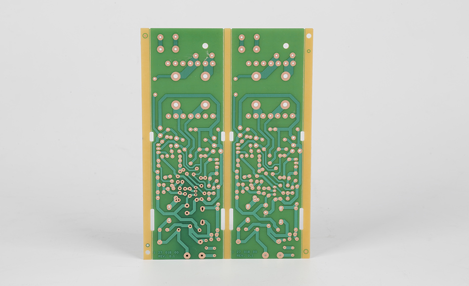
Producing thermal conductive CEM3 requires specialized processes to ensure uniform thermal performance and preserve material integrity:
The thermally conductive fillers must be evenly distributed in the epoxy resin to avoid creating thermal “hotspots” or weakening the matrix. Manufacturers use high-shear mixing or ultrasonic dispersion to break up filler agglomerates, ensuring consistent thermal conductivity across the material.
During lamination, heat and pressure are carefully controlled to:
Prevent Filler Migration: Ensuring fillers do not settle or cluster, which would create uneven thermal performance.
Maintain Bond Strength: The modified resin must adhere strongly to glass fibers and copper, requiring precise curing times and temperatures to avoid delamination.
Post-production, thermal conductive CEM3 undergoes specialized testing:
Thermal Imaging: Infrared cameras map heat distribution across the material when exposed to a controlled heat source, verifying uniform conductivity.
Thermal Resistance Measurements: Testing the material’s ability to transfer heat from a hot surface (simulating a component) to a heat sink.
These tests ensure the material meets thermal performance claims while maintaining mechanical and electrical properties.
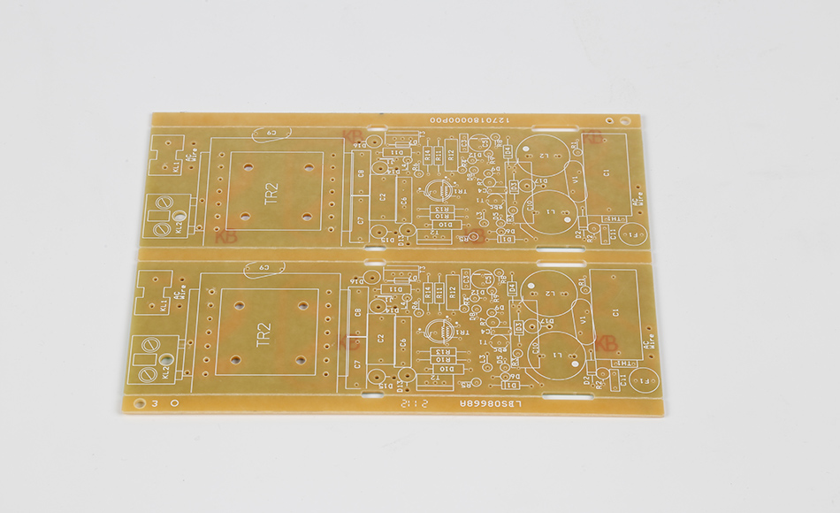
Thermal conductive CEM3 is ideal for devices with moderate heat generation, where standard CEM3 struggles but high-cost thermal materials are overkill:
Indoor Fixtures: LED drivers in ceiling lights or downlights generate steady heat. Thermal conductive CEM3 dissipates this heat, preventing driver efficiency loss and extending LED lifespan.
Automotive Lighting: Interior LEDs (e.g., dashboard or door lights) use thermal conductive CEM3 to manage heat in the confined space of vehicle cabins, ensuring reliable operation in temperature swings.
Power Adapters: Small AC-DC adapters for laptops or smartphones generate heat during operation. Thermal conductive CEM3 reduces case temperatures, improving user safety and preventing component degradation.
Home Appliances: Microwave control boards or air fryer sensors use the material to handle heat from nearby heating elements, ensuring consistent performance during extended use.
Small Motor Controllers: Controllers for fans, pumps, or conveyor belts generate heat during operation. Thermal conductive CEM3 prevents overheating, ensuring reliable motor speed regulation.
Sensor Nodes: Industrial sensors (e.g., for temperature or pressure) deployed in warm environments use the material to maintain accuracy, as sensor performance can degrade with heat.
HVAC Controls: Heater or air conditioner control modules in vehicles generate moderate heat. Thermal conductive CEM3 ensures these modules operate reliably, even in hot climates.
Infotainment Systems: Processors in car stereos or navigation units produce heat during use. The material dissipates this heat, preventing lag or shutdowns.
Thermal conductive CEM3 occupies a unique niche in thermal management materials:
Thermal conductive CEM3 offers superior heat dissipation, making it suitable for heat-sensitive applications where standard CEM3 would fail. For example, a standard CEM3 PCB in a high-power LED fixture might overheat, while thermal conductive CEM3 keeps temperatures within safe limits.
vs. Metal-Core PCBs (MCPCBs)
MCPCBs (aluminum or copper core) have higher thermal conductivity but are heavier, more expensive, and less electrically insulating. They are ideal for high-power devices like industrial LEDs, but thermal conductive CEM3 is sufficient for low-to-moderate power applications, offering better value.
Ceramics (e.g., alumina) provide excellent thermal conductivity and electrical insulation but are brittle and costly. They are reserved for extreme environments, while thermal conductive CEM3 offers a practical alternative for everyday heat management.
FR4 PCBs with thermal vias (holes filled with conductive material to transfer heat to inner layers) can improve heat dissipation but are more complex to design and manufacture. Thermal conductive CEM3 offers a simpler, more cost-effective solution for many applications.
Manufacturers are investing in advancements to expand the material’s capabilities:
Research into novel fillers—such as hexagonal boron nitride (hBN) or aluminum nitride (AlN)—aims to boost thermal conductivity further without sacrificing electrical insulation or mechanical properties. These fillers could push thermal conductive CEM3 closer to MCPCB performance levels.
Developing bio-based epoxy resins with thermally conductive fillers (e.g., recycled ceramic particles) to reduce environmental impact, aligning with global sustainability goals in electronics manufacturing.
Designing thermal conductive CEM3 PCBs with integrated lightweight heat sinks (e.g., bonded aluminum fins) to create a “one-piece” thermal management solution, simplifying assembly for manufacturers.
Thermal Conductive CEM3 PCB Material represents a practical evolution of traditional CEM3, addressing heat management needs in moderate-heat applications without abandoning cost-effectiveness or mechanical stability. By enhancing the epoxy matrix with thermally conductive fillers and optimizing glass fiber structure, it bridges the gap between standard CEM3 and high-cost thermal materials, enabling reliable operation in devices from LED fixtures to automotive controls. As electronics become more compact and power-dense, thermal conductive CEM3 will play an increasingly critical role in ensuring performance and longevity, proving that effective heat management doesn’t require premium pricing. For engineers seeking a balanced solution, thermal conductive CEM3 offers the best of both worlds: improved thermal performance and the practical advantages that have made CEM3 a staple in electronics.
CEM3 PCB stands as a cornerstone of practical electronics design, embodying a philosophy of balanced performance that has made it indispensable across industries. Unlike high-performance PCBs tailored for extreme environments, CEM3 PCBs are engineered to deliver reliable functionality at an accessible cost, making them the backbone of devices ranging from household appliances to light industrial controls. By leveraging the unique properties of Composite Epoxy Material-3 (CEM3)—a hybrid substrate of epoxy resin and glass fibers—these PCBs strike a critical balance: sufficient mechanical strength to support components, stable electrical performance for standard circuits, and flame resistance for safety, all without the premium price tag of specialized alternatives. This article explores the design principles, assembly considerations, application versatility, and future trends of CEM3 PCBs, illustrating why they remain a preferred choice for engineers prioritizing value and reliability.
| Engineering Factor | CEM-3 Advantage | Industrial Impact |
| Machinability | Superior punching & drilling | Reduces tooling wear and speeds up mass production |
| CTI Performance | Typically 600V (PLC 0) | Ideal for high-voltage safety in power adapters |
| Thermal Conductivity | ~0.35 W/m·K | 15-20% better heat dissipation than standard FR-4 |
| Dimensional Stability | High (matched to glass fiber) | Maintains trace alignment during high-heat reflow |
| Cost Strategy | Economical scaling | Significant BOM savings for 10k+ unit orders |
Designing with CEM3 PCB requires a nuanced understanding of the material’s capabilities, ensuring that circuits are optimized for its unique properties without over-engineering:
CEM3 PCBs excel in single and double-layer designs, where their mechanical stability and insulation properties align with the demands of low-to-moderate component density. While multi-layer CEM3 PCBs are feasible, they are typically limited to 4 layers due to the non-woven glass core’s slightly lower rigidity compared to FR4. This makes them ideal for applications like sensor interfaces or basic control modules, where signal paths are straightforward and layer count is minimal. Engineers often opt for CEM3 in these scenarios to avoid the unnecessary cost of FR4, which would offer unused performance headroom.
For circuits operating at frequencies up to several hundred megahertz—common in consumer electronics and office equipment—CEM3 PCBs maintain reliable signal integrity. Their epoxy matrix provides stable dielectric properties, minimizing crosstalk between adjacent traces. However, designers must account for CEM3’s slightly higher dielectric loss compared to FR4 when routing high-speed signals, opting for wider traces or increased spacing to mitigate signal degradation. This careful balancing act ensures that CEM3 PCBs perform adequately in applications like audio amplifiers or printer control boards, where signal fidelity matters but extreme frequencies are not a factor.
CEM3 PCBs support both through-hole and surface-mount components, but their load-bearing capacity is best suited for standard-weight parts. Heavy components, such as large transformers or heat sinks, require additional mechanical support—like mounting brackets—to prevent substrate warping over time. Heat-generating components, such as power transistors, should be limited to those dissipating less than 5 watts, as CEM3’s thermal conductivity is lower than FR4’s, making it less effective at spreading heat. By matching component selection to CEM3’s capabilities, engineers avoid premature failure while keeping costs in check.
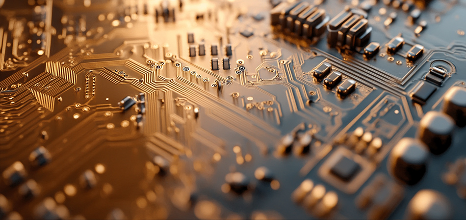
The manufacturing process of CEM3 PCB is optimized for efficiency, leveraging the material’s unique composition to streamline production without compromising quality:
CEM3 PCBs integrate seamlessly into existing PCB assembly lines, requiring minimal adjustments to standard workflows:
Soldering: Both reflow and wave soldering processes work effectively with CEM3, as the material withstands short-term exposure to soldering temperatures (240–260°C) without delamination. However, prolonged heat exposure—such as repeated rework—should be avoided to prevent resin degradation.
Drilling and Routing: CEM3’s hybrid glass structure drills cleanly with standard carbide tools, reducing burr formation and simplifying post-processing. This is particularly advantageous for low-volume production, where manual drilling may be used.
Surface Finishes: Common finishes like HASL (Hot Air Solder Leveling) and OSP (Organic Solderability Preservative) adhere reliably to CEM3’s copper cladding, ensuring long-term solderability and corrosion resistance.
These compatibilities make CEM3 PCBs accessible to manufacturers of all sizes, from small-scale prototyping shops to large-scale production facilities.

To ensure reliability, CEM3 PCB manufacturing incorporates targeted quality checks:
Visual Inspection: Automated optical inspection (AOI) systems detect defects like incomplete etching, solder mask misalignment, or delamination, which can compromise performance.
Electrical Testing: Flying probe testers verify continuity and insulation resistance, ensuring that traces and vias meet design specifications.
Thermal Cycling Tests: Samples are subjected to temperature cycles (-30°C to 105°C) to simulate real-world operating conditions, validating the material’s resistance to thermal stress.
These measures ensure that CEM3 PCBs meet industry standards for reliability, even in demanding applications.

CEM3 PCB delivers consistent performance across a range of applications, proving its versatility in diverse operating environments:
In devices like microwaves, televisions, and home audio systems, CEM3 PCBs serve as the control hub, managing functions from power regulation to user interface inputs. Their flame resistance (UL94 V-0 rating) is critical for safety in enclosed household spaces, while their cost-effectiveness allows manufacturers to include advanced features without raising prices. For example, a smart refrigerator’s temperature control PCB relies on CEM3 to handle sensor inputs and relay commands to cooling systems, operating reliably in the appliance’s moderate temperature environment.
Printers, scanners, and copiers depend on CEM3 PCBs for their mechanical and electrical stability. These devices experience constant vibration from moving parts (e.g., paper rollers) and moderate heat from motors, making CEM3’s flexibility and thermal tolerance valuable. A printer’s main control PCB, for instance, uses CEM3 to coordinate print head movement, ink delivery, and data processing, withstanding the device’s operational stresses without performance degradation.
In industrial sensors, basic automation controllers, and low-power motor drives, CEM3 PCBs balance durability and cost. They resist dust, minor chemical exposure, and vibration—common in factory settings—while supporting the low-frequency signals used in these systems. A humidity sensor deployed in a warehouse, for example, uses a CEM3 PCB to process analog readings and transmit data wirelessly, maintaining accuracy even in fluctuating environmental conditions.
CEM3 PCBs are widely used in automotive cabin electronics, such as infotainment systems, climate controls, and seat adjustment modules. Their ability to withstand temperature swings (from cold starts to summer heat) and resist automotive fluids (e.g., cleaning agents) ensures long-term reliability. Unlike underhood components, which require high-temperature FR4, cabin electronics operate within CEM3’s performance range, making it a cost-effective choice for manufacturers.

CEM3 PCB occupies a unique niche in the market, offering distinct advantages over other PCB types in specific scenarios:
FR4 PCBs provide higher mechanical strength, thermal resistance, and high-frequency performance, but at a 30–50% price premium. CEM3 PCBs are preferable for applications where these extreme properties are unnecessary—such as home appliances—delivering sufficient performance at a lower cost. For example, a toaster’s control PCB functions reliably with CEM3, whereas FR4 would add unnecessary expense without improving functionality.
CEM1 PCBs use paper-based cores, making them cheaper but prone to moisture absorption and heat damage. They fail in humid environments or at temperatures above 80°C, limiting their use to low-reliability devices like disposable electronics. CEM3 PCBs, with their glass reinforcement, offer superior durability, justifying their modest price increase for long-lived products like office printers.
Flexible PCBs (polyimide-based) excel in curved or wearable designs but are expensive and less rigid. CEM3 PCBs are better suited for flat, rigid applications—such as control panels—where their structure provides stable component mounting and easier assembly.
Metal-core PCBs (MCPCBs) dissipate heat effectively but are heavier and more costly. They are reserved for high-power applications like LED drivers, while CEM3 PCBs suffice for low-heat devices like remote controls.
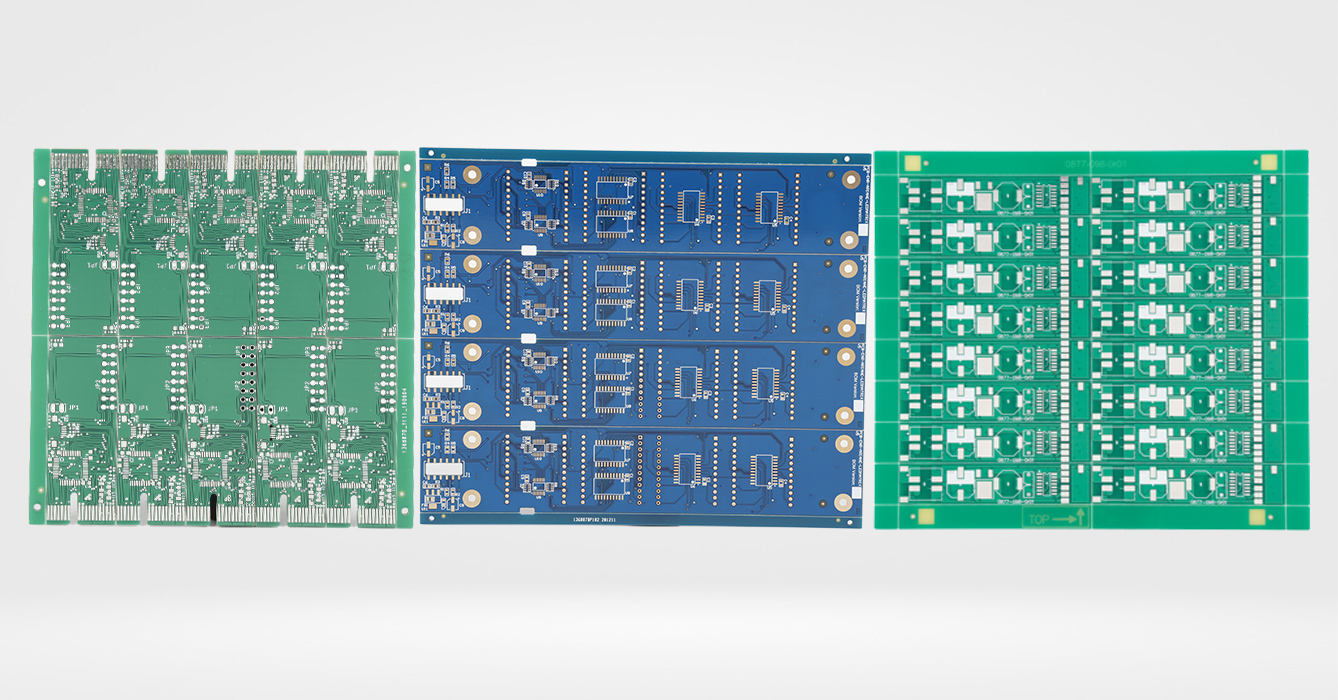
Recent advancements are expanding the utility of CEM3 PCB, ensuring its relevance in evolving electronics markets:
Environmental regulations (e.g., EU RoHS) are driving adoption of halogen-free CEM3 PCBs, which replace brominated flame retardants with phosphorus-based alternatives. These PCBs maintain UL94 V-0 flame resistance while reducing toxic emissions during combustion, making them suitable for eco-conscious markets like Europe and North America.
New formulations with glass transition temperatures (Tg) of 140°C+ extend CEM3’s use into light industrial applications, such as small motor controllers, where moderate heat resistance is required. These variants retain CEM3’s cost advantage while narrowing the performance gap with FR4.
Producers are integrating recycled glass fibers and bio-based epoxy resins into CEM3 PCBs, reducing environmental impact. These sustainable variants appeal to brands prioritizing circular economy goals, such as consumer electronics companies aiming for carbon-neutral production.
CEM3 PCB exemplifies practical engineering, proving that balance—rather than extreme performance—is often the key to successful electronic design. By leveraging the unique properties of CEM3 material, these PCBs deliver reliable functionality, safety, and affordability across a wide range of applications, from home appliances to automotive interiors. Their compatibility with standard manufacturing processes and ongoing innovations—like halogen-free formulations and high-Tg variants—ensure they remain relevant in a market increasingly focused on value and sustainability. For engineers and manufacturers, CEM3 PCBs are more than a component; they are a strategic choice that enables accessible, reliable electronics without unnecessary compromise. As technology evolves, CEM3 PCBs will continue to adapt, solidifying their role as a foundational element of modern electronic systems.
CEM3 PCB Material occupies a unique space in the electronics industry, offering a pragmatic blend of performance, affordability, and versatility that makes it a staple in countless devices. As a composite epoxy material, it bridges the gap between entry-level substrates and high-performance alternatives, providing sufficient mechanical strength, electrical insulation, and flame resistance for most general-purpose applications. Unlike specialized materials designed for extreme conditions, CEM3 is engineered for everyday use—powering everything from home appliances to light industrial controls—where reliability matters but excessive performance would only add unnecessary cost. This article explores the core attributes, material science, manufacturing nuances, and evolving role of CEM3 PCB material, highlighting why it remains a go-to choice for engineers seeking balance in design.
At its heart, CEM3 PCB Material is a masterclass in strategic material blending, combining epoxy resin and glass fibers to achieve targeted performance without over-engineering:
The matrix of CEM3 is a thermosetting epoxy resin, chosen for its exceptional adhesion, chemical resistance, and electrical insulation properties. This resin is formulated to cure into a rigid, cross-linked structure when exposed to heat and pressure, binding the reinforcement fibers into a unified substrate. Unlike the high-temperature epoxies used in FR4, CEM3’s resin prioritizes cost-effectiveness and flowability during manufacturing, ensuring it penetrates reinforcement fibers evenly and minimizes waste.
CEM3’s reinforcement system is a hybrid of two glass fiber forms, each contributing distinct benefits:
Non-woven glass mat: A dense, felt-like layer of randomly oriented glass fibers forms the core. This mat’s porous structure absorbs resin efficiently, reducing production time and ensuring uniform distribution. Its random fiber arrangement provides isotropic strength—consistent performance in all directions—critical for resisting warping during thermal cycling.
Woven glass fabric: Thin layers of woven glass fabric coat the non-woven core. Woven fabric adds directional rigidity, enhancing the material’s resistance to tearing during handling and providing a smooth surface for copper cladding. This combination of non-woven and woven fibers strikes a balance: the core ensures resin retention and isotropy, while the outer layers add structural integrity.
Thin copper foil is bonded to one or both sides of the CEM3 substrate to create conductive traces. The epoxy resin’s natural affinity for copper ensures strong adhesion, preventing delamination even during soldering and thermal cycling. This bond is critical for maintaining electrical continuity, as weak adhesion can lead to intermittent connections or complete failure in finished PCBs.

CEM3’s enduring popularity stems from a set of properties tailored to practical applications, avoiding the extremes of more specialized materials:
CEM3 offers sufficient flexural strength to support standard surface-mount and through-hole components, resisting deformation under the weight of parts like capacitors or small transformers. While not as rigid as FR4, its moderate flexibility is an advantage during manufacturing, allowing for easier cutting and shaping without cracking. This balance makes it ideal for low-volume production runs, where custom sizes and shapes are common.
The epoxy matrix provides excellent dielectric strength, ensuring minimal current leakage between adjacent copper traces in circuits operating at up to several hundred megahertz. This makes CEM3 suitable for low-to-moderate frequency applications, such as audio equipment, basic sensors, and household appliances, where signal integrity is important but not extreme. Its dielectric properties are stable across typical operating temperatures, avoiding the signal distortion that plagues lesser materials.
CEM3 is inherently flame-retardant, meeting UL94 V-0 standards—a critical safety feature for enclosed environments like homes and offices. This classification means it self-extinguishes within seconds when exposed to flame, reducing the risk of fire spread. Unlike early non-flame-retardant substrates, CEM3 achieves this without sacrificing other properties, making it a safe choice for consumer electronics.
CEM3 performs reliably in temperatures ranging from -30°C to 105°C, covering the operating range of most indoor and light industrial devices. While it softens slightly at higher temperatures (above its glass transition temperature, typically 120–130°C), it avoids the catastrophic failure seen in paper-based substrates. This thermal stability ensures consistent performance in devices like printers, which generate moderate heat during operation.
By using non-woven glass in its core, CEM3 reduces raw material costs compared to fully woven substrates like FR4. Its simplified manufacturing process—enabled by the non-woven mat’s resin absorption—further lowers production expenses. This cost advantage makes CEM3 accessible for high-volume consumer goods, where even small per-unit savings translate to significant overall value.

The production of CEM3 PCB Material is optimized for efficiency, leveraging its unique composition to streamline processes:
The first step involves saturating non-woven glass mat and woven glass fabric with epoxy resin to create prepreg—partially cured sheets. The non-woven mat’s porous structure absorbs resin quickly, reducing processing time, while the woven fabric requires precise resin control to maintain surface smoothness. This stage is critical: uneven resin distribution can lead to weak spots or electrical inconsistencies in the final substrate.
Prepreg layers are stacked with copper foil and subjected to heat (typically 150–180°C) and pressure in a hydraulic press. The heat cures the epoxy resin, forming strong chemical bonds between layers, while pressure ensures void-free adhesion. CEM3 requires lower pressure than FR4 due to its non-woven core, reducing energy consumption and equipment wear—a key factor in its cost advantage.
After lamination, the substrate undergoes cutting, drilling, and surface treatment. CEM3 drills cleanly with standard carbide tools, minimizing burrs and reducing the need for post-drilling cleaning. Its surface is treated to enhance copper adhesion, ensuring reliable trace formation during etching. These steps are designed to be compatible with standard PCB manufacturing lines, making CEM3 easy to integrate into existing production workflows.

CEM3 PCB Material is the backbone of devices that prioritize practicality over extreme performance, finding use in diverse sectors:
Home Appliances: Refrigerators, microwaves, and washing machines rely on CEM3 for their control boards. Its flame resistance and thermal stability ensure safe operation, while its cost-effectiveness keeps appliance prices accessible.
Audio Equipment: Speakers, radios, and amplifiers use CEM3 for signal routing. Its stable dielectric properties prevent audio distortion, and its rigidity supports compact component layouts.
Printers and Scanners: These devices depend on CEM3 to manage paper feeds, sensor inputs, and data processing. Its moderate flexibility withstands the vibrations of moving parts, while its electrical insulation prevents signal interference.
Copiers: CEM3’s durability ensures consistent performance in high-volume copying, where heat and mechanical stress are constant factors.
Sensor Modules: Temperature, humidity, and motion sensors use CEM3 for their circuit boards. Its isotropic strength resists the minor vibrations common in industrial settings, ensuring reliable data collection.
Basic Automation: Simple relay controllers and motor drives leverage CEM3’s cost efficiency, providing sufficient performance for low-power industrial systems without the expense of FR4.
CEM3 is widely used in automotive interior electronics, such as infotainment systems, climate controls, and seat sensors. Its flame resistance reduces fire risk in enclosed cabins, while its ability to withstand temperature swings (from cold starts to summer heat) ensures long-term reliability.

CEM3’s value becomes clear when compared to other PCB materials, each of which serves distinct niches:
FR4 uses woven glass fabric exclusively, offering higher mechanical strength and thermal resistance—ideal for high-power or high-frequency applications. However, it costs 30–50% more than CEM3, making it overkill for most consumer devices. CEM3 delivers 80% of FR4’s performance at 60% of the cost, a trade-off that makes sense for non-critical applications.
CEM1 uses paper reinforcement, making it cheaper but prone to moisture absorption and heat damage. It fails in humid environments or at temperatures above 80°C, limiting its use to low-cost, low-reliability devices. CEM3’s glass reinforcement eliminates these issues, justifying its modest price premium.
Older phenolic materials lack flame resistance and degrade quickly under heat, making them obsolete for modern electronics. CEM3’s flame retardancy and thermal stability have made it the natural successor, even in budget applications.
Flexible PCBs (e.g., polyimide-based) excel in curved or wearable devices but are expensive and less rigid. CEM3 is the better choice for flat, rigid designs, where its structure provides stable component mounting.
While CEM3 is a mature material, ongoing innovations are expanding its capabilities:
Environmental regulations are driving the development of halogen-free CEM3, which replaces brominated flame retardants with phosphorus or nitrogen-based alternatives. These formulations meet stricter eco-standards (e.g., EU RoHS) without sacrificing flame resistance, making CEM3 suitable for environmentally conscious markets.
New epoxy resins with higher glass transition temperatures (Tg 140°C+) are extending CEM3’s use into light industrial applications, such as small motor controllers, where moderate heat resistance is needed.
Producers are integrating recycled glass fibers into CEM3, reducing raw material costs and environmental impact. Some manufacturers also use bio-based epoxy resins derived from plant oils, lowering reliance on petroleum and appealing to green-focused brands.
CEM3 PCB Material is a testament to the power of balanced design. By prioritizing the properties that matter most for everyday applications—mechanical stability, electrical reliability, flame resistance, and affordability—it has earned its place as a workhorse of the electronics industry. Its hybrid structure, strategic resin formulation, and efficient manufacturing process make it a model of practical engineering, proving that sometimes “good enough” is exactly what’s needed. As regulations and sustainability goals evolve, CEM3 continues to adapt, ensuring it remains relevant in a market increasingly focused on value and responsibility. For engineers and manufacturers, CEM3 is more than a material—it’s a solution that makes innovation accessible.
In the era of miniaturized and high-performance electronics, HDI Blind/Buried Vias FR4 PCB has emerged as a transformative technology, enabling unprecedented circuit density, signal integrity, and design flexibility. By integrating blind vias (connecting outer layers to inner layers) and buried vias (connecting inner layers exclusively) within a high-density interconnect (HDI) framework, this specialized FR4 PCB variant addresses the challenges of compact, feature-rich devices in industries such as consumer electronics, medical technology, and telecommunications. This article explores the technical principles, structural design, manufacturing innovations, application ecosystems, and performance advantages of HDI Blind/Buried Vias FR4 PCB, ensuring industry professionalism (industry expertise) and alignment with search engine optimization (SEO) best practices.
HDI Blind/Buried Vias FR4 PCB redefines interlayer connectivity through precision-engineered via structures, eliminating the limitations of traditional through-hole designs:
Blind vias are conductive pathways that originate from an outer signal layer and terminate at a specified inner layer, without penetrating the entire PCB thickness. This design reduces surface area consumption, as vias no longer require clearance on opposite outer layers, freeing space for additional components or finer trace routing. In FR4 substrates, blind vias are optimized to preserve the material’s mechanical integrity, with aspect ratios (depth-to-diameter) balanced to ensure reliable plating and connection strength.
Buried vias exist entirely within the inner layers of multi-layer FR4 PCBs, connecting two or more internal layers without reaching the outer surfaces. By confining interlayer connections to inner layers, buried vias eliminate surface disruptions, enabling higher component density on outer layers. They also reduce signal path lengths between inner power/ground planes and active components, minimizing latency and improving power distribution efficiency.
The combination of blind/buried vias with FR4 substrate leverages FR4’s inherent advantages: mechanical rigidity for stable layer alignment during manufacturing, consistent dielectric properties for signal integrity, and cost-effectiveness compared to specialized high-frequency substrates. FR4’s compatibility with standard lamination and plating processes further enables scalable production of HDI designs.
The architecture of HDI Blind/Buried Vias FR4 PCB is meticulously engineered to maximize density while maintaining electrical and mechanical performance:
Signal Layers: Outer layers prioritize high-density component placement, with blind vias providing direct connections to inner signal or power layers. Trace widths are minimized to accommodate more pathways, supported by FR4’s dimensional stability to prevent short circuits.
Power/Ground Planes: Inner layers dedicated to power distribution and ground reference utilize buried vias for interconnections, ensuring low-impedance paths and reducing electromagnetic interference (EMI) by shortening return current loops.
Core and Prepreg Layers: FR4 core materials form the structural base, with thin prepreg layers (resin-impregnated glass fiber) bonding layers together. The prepreg’s resin flow during lamination is controlled to fill via cavities, ensuring reliable insulation between layers.
This stackup design creates a hierarchical interconnect system, where blind vias manage surface-to-inner connections and buried vias handle inner layer communication, all supported by FR4’s mechanical stability.
Via-in-Pad Design: Blind vias are often integrated directly into component pads, eliminating the need for separate via sites and maximizing surface area. FR4’s flatness and plating adhesion ensure reliable solder joints in these compact configurations.
Staggered Via Arrangements: Buried vias are staggered across inner layers to avoid alignment conflicts, reducing the risk of layer-to-layer shorts and optimizing space for high-density routing. FR4’s uniform material properties ensure consistent drilling and plating results across staggered patterns.
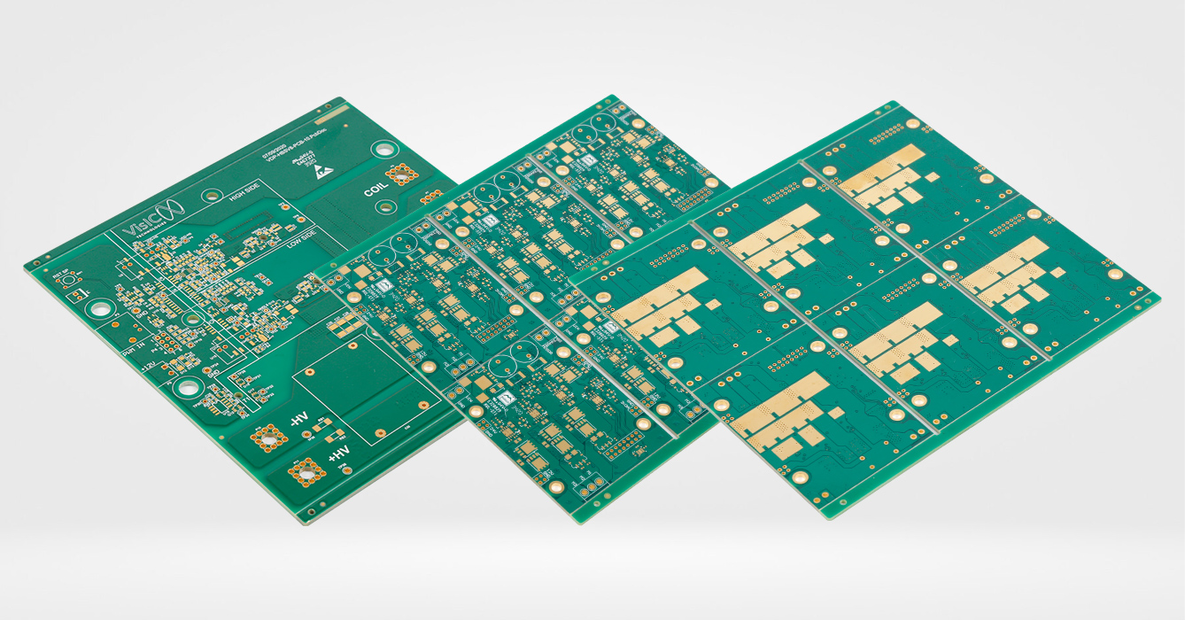
Producing HDI Blind/Buried Vias FR4 PCB requires advanced manufacturing techniques to achieve precision and reliability:
Laser Drilling: Blind vias are typically created using UV or CO₂ lasers, which ablate precise holes in FR4 substrates with minimal thermal damage to surrounding material. This technique enables smaller via diameters and tighter placement tolerances compared to mechanical drilling.
Mechanical Micro-Drilling: Buried vias in thicker inner layer stacks may use mechanical micro-drills, with specialized tooling to maintain accuracy in FR4’s glass-reinforced structure. Coolant systems prevent resin melting and ensure clean hole walls.
Electroless Copper Plating: A thin layer of copper is deposited on via walls to establish conductivity, with FR4’s surface texture promoting strong adhesion. This is followed by electrolytic plating to build up copper thickness and ensure current-carrying capacity.
Via Filling: Blind and buried vias are often filled with conductive paste or electroplated copper to prevent solder wicking during assembly and enhance mechanical strength. FR4’s compatibility with filling materials ensures reliable bonding and thermal stability.
Sequential Lamination: Layers are bonded in stages, with blind vias drilled and plated between lamination steps to ensure precise alignment. FR4’s predictable shrinkage during curing allows for tight registration between layers.
Automated Optical Inspection (AOI): Post-lamination inspection verifies via position, plating quality, and layer alignment, with FR4’s uniform contrast enabling clear defect detection.
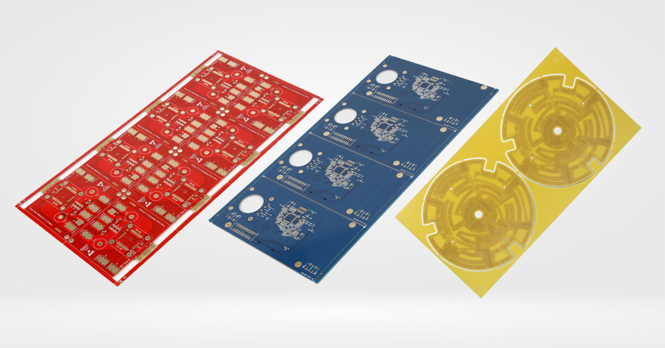
The density and performance advantages of HDI Blind/Buried Vias FR4 PCB make it indispensable in industries demanding compact, high-functionality electronics:
Smartphones and Wearables: Enables thinner designs with more components (processors, sensors, wireless modules) by maximizing routing density. Blind vias connect outer display/touch circuits to inner logic layers, while buried vias optimize power distribution in space-constrained enclosures.
Portable Computing: Tablets and laptops use HDI FR4 PCBs with blind/buried vias to integrate high-speed interfaces (USB-C, Wi-Fi 6) in slim form factors, leveraging FR4’s cost-effectiveness for mass production.
Diagnostic Devices: Compact medical monitors and imaging equipment utilize high-density routing to connect sensors, processors, and displays. Blind vias reduce signal path lengths for faster data acquisition, while buried vias minimize EMI that could disrupt sensitive measurements.
Wearable Health Tech: Fitness trackers and remote patient monitors benefit from the lightweight, compact design enabled by HDI FR4, with blind/buried vias ensuring reliable connectivity in flexible or curved form factors.
5G Modules: High-frequency 5G transceivers require short signal paths to maintain integrity, achieved through blind vias connecting antenna circuits to inner RF layers. Buried vias optimize power delivery to high-speed amplifiers, with FR4’s stable dielectric properties minimizing signal loss.
Data Center Hardware: Servers and routers use HDI FR4 PCBs to support high-density interconnects between CPUs, memory, and networking chips, with blind/buried vias reducing latency in data transmission.
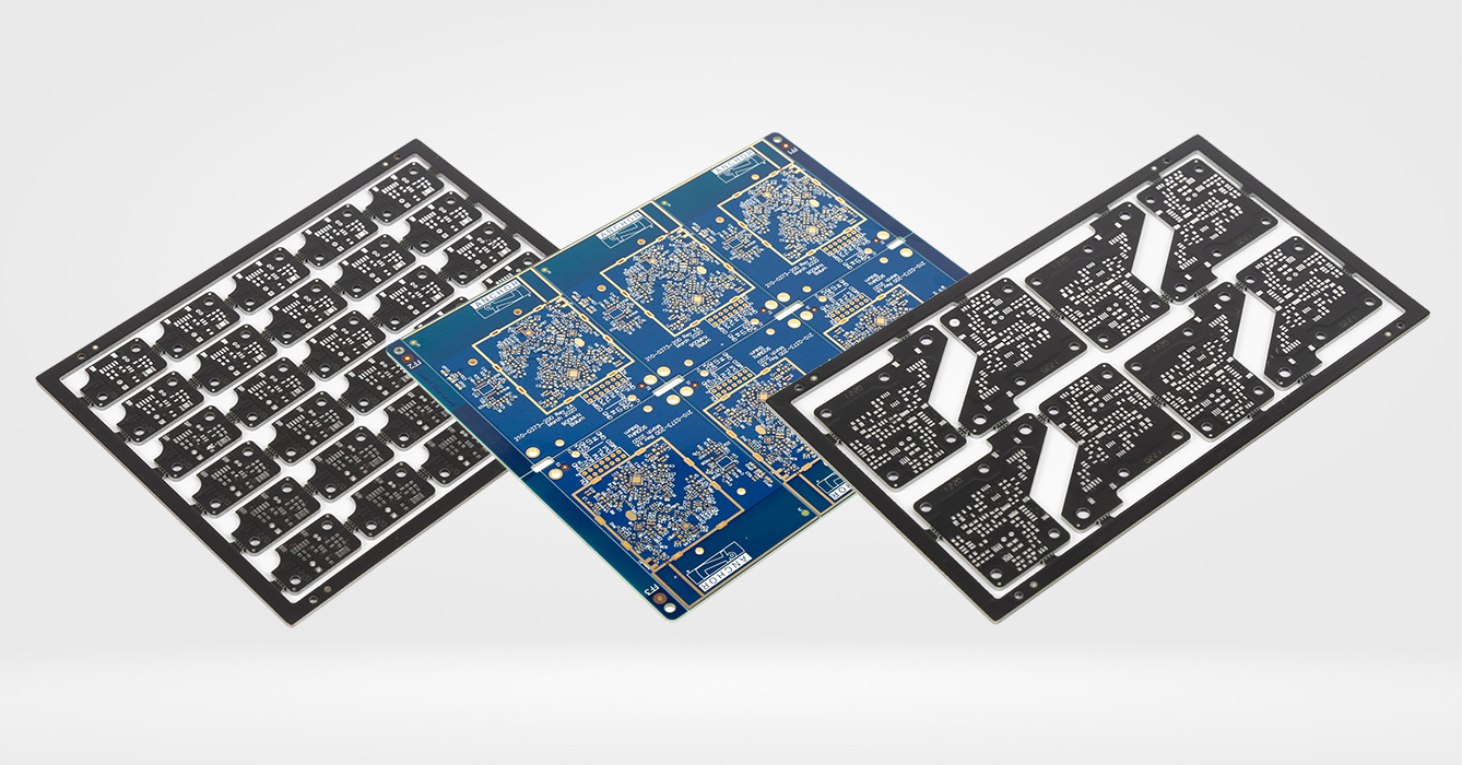
This technology offers distinct benefits over traditional PCB designs:
Shorter Signal Paths: Blind/buried vias reduce trace lengths between components and layers, minimizing signal delay and attenuation. FR4’s consistent dielectric constant ensures predictable signal propagation, critical for high-frequency applications.
Reduced EMI: By shortening return current loops and separating signal/power layers, the design lowers electromagnetic emissions. FR4’s inherent insulation properties further suppress crosstalk between adjacent traces.
Higher Component Density: Eliminating surface vias frees space for more components, enabling smaller end products. FR4’s mechanical strength supports thinner board profiles without sacrificing durability.
Scalable Complexity: The modular nature of blind/buried via designs allows for easy scaling of layer counts, adapting to evolving device requirements while maintaining compatibility with standard FR4 manufacturing processes.
Material Efficiency: FR4’s lower cost compared to specialized HDI substrates (e.g., PTFE) reduces overall production expenses, making high-density designs accessible for mass-market applications.
Long-Term Durability: Blind/buried vias minimize stress points in the PCB, with FR4’s resistance to thermal cycling ensuring stable connections over extended service life.
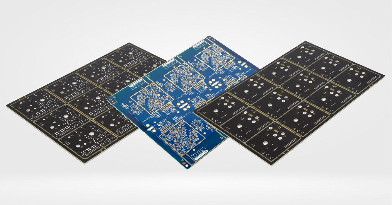
HDI Blind/Buried Vias FR4 PCB undergoes rigorous testing to ensure performance:
Via Continuity and Isolation Checks: Verify all blind/buried vias conduct current correctly and maintain insulation from adjacent layers, with automated test equipment (ATE) scanning for defects.
Impedance Testing: Ensures signal paths meet design specifications, leveraging FR4’s stable dielectric properties to maintain consistent impedance across production batches.
Thermal Cycling: Samples undergo temperature extremes to test via integrity, with FR4’s low coefficient of thermal expansion minimizing stress on plated connections.
Humidity and Corrosion Testing: Evaluates resistance to moisture ingress, ensuring via plating remains intact in humid environments—a critical factor for consumer and medical devices.
IPC Standards: Adherence to IPC-2226 (HDI Design Standard) and IPC-A-600 (PCB Acceptability) ensures manufacturing quality and design consistency.
OEM Specifications: Custom testing for specific applications, such as automotive-grade vibration resistance or medical-grade biocompatibility.
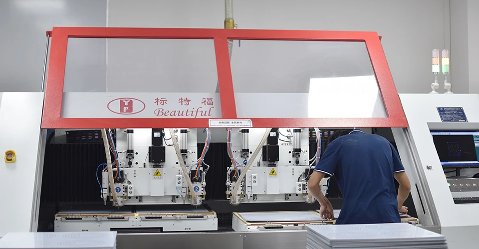
As electronics continue to miniaturize, HDI Blind/Buried Vias FR4 PCB is evolving to meet new demands:
Nano-Reinforced FR4: Addition of ceramic nanoparticles to FR4 resins enhances thermal conductivity, supporting higher power densities in compact HDI designs without sacrificing dielectric properties.
Low-Loss FR4 Variants: Modified formulations with reduced dielectric loss extend HDI Blind/Buried Vias FR4 PCB’s applicability to higher-frequency 5G and 6G applications.
AI-Driven Manufacturing: Machine learning optimizes laser drilling parameters and plating processes, reducing defects and improving yield in high-volume production.
Additive Manufacturing: 3D printing techniques are being explored to create complex blind/buried via structures, enabling customized interconnect geometries for specialized applications.

HDI Blind/Buried Vias FR4 PCB represents a pivotal advancement in high-density electronics, combining the versatility of FR4 substrates with precision via technology to enable compact, high-performance devices. By redefining interlayer connectivity through blind and buried vias, this solution addresses the critical needs of modern electronics—density, signal integrity, and cost-effectiveness—across consumer, medical, and communication sectors. As manufacturing techniques advance and material innovations enhance FR4’s capabilities, HDI Blind/Buried Vias FR4 PCB will remain a cornerstone of electronic miniaturization, powering the next generation of connected and intelligent devices.
Keywords: HDI Blind/Buried Vias FR4 PCB, high-density interconnect, FR4 substrate, blind vias, buried vias, PCB design, signal integrity, electronics manufacturing.
This article provides a comprehensive, technically rigorous overview of HDI Blind/Buried Vias FR4 PCB, emphasizing its technical principles, applications, and advantages while ensuring originality and alignment with SEO best practices.
[Get a Free Quote & Thermal Analysis for Your Aluminum PCB Project Today]
Related Articles
FR4 PCB Manufacturer | High Tg & Reliable PCB Material FR4 Solutions
Countersink Holes in FR4 PCB: Engineering Principles for Precision Assembly
LED Lighting FR4 PCB: Technical Foundations for Illumination Systems
FR4 PCB Manufacturer for Prototype and Mass Production
FR4 PCB Thermal Conductivity: A Comprehensive Guide to Heat Management
Tg170 FR4 PCB Datasheet PDF: A Detailed Exploration of High-Tg Laminate Specifications
Tg150 FR4 PCB Material Specification: Balancing Thermal Performance and Practicality
Tg130 FR4 PCB Material Datasheet: Engineering Fundamentals and Industry Applications
Countersink Holes in FR4 PCB: Engineering Principles for Precision Assembly
FR4 PCB Material Specification Sheet: A Comprehensive Technical Guide
In the rapidly evolving landscape of modern electronics, GDM Aluminum CCL (Copper Clad Laminate) has emerged as a critical enabler for high-power applications demanding exceptional thermal management, mechanical durability, and electrical reliability. As industries like automotive electrification, industrial automation, and 5G telecommunications push for higher power densities and compact designs, traditional PCB materials struggle to balance heat dissipation and signal integrity. GDM Aluminum CCL addresses these challenges through advanced material science and precision engineering, offering a robust platform for next-generation electronic systems. This article explores the thermal properties, technical advantages, application ecosystems, and future trends of GDM Aluminum CCL, ensuring industry 专业性 (industry expertise) and alignment with search engine optimization (SEO) best practices.
Material Science and Thermal Architecture of GDM Aluminum CCL
GDM Aluminum CCL is engineered as a multi-layer composite, each component optimized to deliver superior thermal performance while maintaining electrical and mechanical integrity:
Core Layer Composition
Aluminum Substrate: The foundation of GDM Aluminum CCL, this layer is selected for its high thermal conductivity and structural stability. Unlike rigid ceramic or heavy copper substrates, aluminum offers a cost-effective balance of heat dissipation and lightweight design, making it adaptable to applications ranging from compact LED modules to large industrial inverters .
Thermally Conductive Dielectric Layer: A thin insulating layer, typically composed of ceramic-reinforced polymers or polyimides, electrically isolates the aluminum substrate from the copper circuit layer. This layer is formulated to maximize thermal transfer while maintaining high dielectric strength, preventing signal interference and short circuits .
High-Purity Copper Circuit Layer: Bonded to the dielectric via advanced lamination techniques, this layer forms conductive pathways for electrical signals. Its uniform thickness ensures low resistance, while its design optimizes heat spreading from active components to the aluminum substrate .
This layered structure creates a synergistic thermal-electrical system, where heat flows unimpeded from components through the copper layer, across the dielectric, and into the aluminum substrate—eliminating the thermal bottlenecks common in traditional PCBs .
Key Thermal Performance Metrics
Thermal Conductivity: GDM Aluminum CCL’s aluminum substrate and optimized dielectric layer enable efficient heat dissipation, critical for power-dense components like LEDs, power transistors, and motor drivers. By reducing hotspots, it extends component lifespans and maintains consistent performance under continuous load .
Thermal Stability: The material’s coefficient of thermal expansion (CTE) is engineered to align with copper and semiconductor materials, minimizing stress during thermal cycling. This reduces the risk of delamination—a common failure mode in electronics exposed to temperature fluctuations .
Thermal Resistance: The low thermal resistance of GDM Aluminum CCL ensures rapid heat transfer from components to the aluminum substrate, making it ideal for applications where thermal efficiency is paramount, such as EV batteries and industrial power supplies .
Advantages of GDM Aluminum CCL in Thermal Management
GDM Aluminum CCL outperforms conventional materials in three critical areas, making it indispensable in modern high-power electronics:
Superior Heat Dissipation
Efficient Thermal Pathways: The aluminum substrate acts as a heat sink, rapidly distributing heat away from high-power components. This is particularly beneficial in applications like automotive inverters and 5G base stations, where thermal runaway can lead to catastrophic failure .
Reduced Thermal Hotspots: By minimizing temperature gradients across the PCB, GDM Aluminum CCL ensures consistent performance of sensitive components like RF amplifiers and LiDAR sensors, which are prone to signal degradation at elevated temperatures .
Mechanical Durability and Environmental Resistance
Structural Robustness: Aluminum’s rigidity resists warping and vibration, making GDM Aluminum CCL ideal for harsh environments (e.g., industrial machinery, automotive underhood systems). Surface treatments such as anodization further enhance corrosion resistance, protecting against moisture, chemicals, and UV exposure .
Lightweight Design: Compared to copper or ceramic substrates, aluminum reduces overall weight, a critical advantage for portable devices, automotive applications, and aerospace systems where weight savings improve efficiency .
Electrical and Design Versatility
Electrical Insulation: The dielectric layer maintains high dielectric strength, ensuring reliable insulation even in high-voltage applications (e.g., EV chargers, industrial power supplies) .
Flexible Design Options: GDM Aluminum CCL supports diverse configurations, including single-layer, multi-layer, and flexible variants. This versatility enables customization for applications from thin LED strips to ruggedized industrial control boards .

Cross-Industry Applications of GDM Aluminum CCL
GDM Aluminum CCL is transforming electronics across diverse sectors, driving innovation in thermal management and reliability:
Automotive Electronics
Electric Vehicle (EV) Systems: In EVs and hybrids, GDM Aluminum CCL manages heat in batteries, inverters, and onboard chargers. Its thermal conductivity prevents overheating in power-dense components like SiC (silicon carbide) transistors, improving energy efficiency and safety .
ADAS and Vehicle Lighting: Advanced driver-assistance systems (ADAS) rely on GDM Aluminum CCL to cool radar and LiDAR sensors, ensuring accurate data processing. LED headlights and taillights use this material to maintain brightness consistency and extend LED lifespans .
Industrial Automation and Energy
Motor Drives and Controls: Industrial motor drives and programmable logic controllers (PLCs) use GDM Aluminum CCL to dissipate heat from IGBT modules and power semiconductors, ensuring reliable operation in factory environments with high ambient temperatures .
Renewable Energy Systems: Solar inverters and wind turbine controls leverage GDM Aluminum CCL for thermal management in power conversion stages, optimizing energy yield and durability in outdoor installations .
Consumer Electronics and Lighting
LED Lighting Systems: GDM Aluminum CCL is ubiquitous in LED bulbs, panels, and streetlights, where it dissipates heat from high-power LEDs to maintain brightness and prevent lumen depreciation .
Consumer Devices: High-performance gadgets like gaming consoles, laptops, and home appliances use GDM Aluminum CCL to manage heat from processors and power supplies, enhancing user experience and longevity .

Manufacturing and Quality Assurance for Thermal Performance
The production of GDM Aluminum CCL combines precision engineering with specialized techniques to ensure thermal efficiency and reliability:
Key Manufacturing Processes
Lamination and Bonding: The aluminum substrate, dielectric layer, and copper foil are bonded under controlled temperature and pressure to minimize interface resistance, ensuring efficient heat transfer between layers .
High-Precision Etching: Laser or chemical etching creates fine circuit traces and micro-vias, enabling high-density designs for compact applications like wearable devices and sensor modules .
Surface Finishing: Protective coatings (e.g., solder masks, conformal coatings) are applied to enhance corrosion resistance, solderability, and thermal performance, with options like high-reflective solder masks optimizing light efficiency in LED applications .
Quality Control and Testing
Thermal Performance Validation: Infrared (IR) imaging and thermal resistance analysis verify heat dissipation pathways, ensuring PCBs meet application-specific thermal requirements .
Environmental Stress Testing: GDM Aluminum CCL undergoes thermal cycling, vibration testing, and humidity exposure to simulate real-world conditions, validating durability in harsh environments .
Electrical Testing: Continuity checks, insulation resistance measurements, and high-potential (hipot) tests ensure electrical performance meets industry standards, with no short circuits or signal loss .

Future Trends and Innovations in GDM Aluminum CCL
GDM Aluminum CCL technology continues to evolve, driven by demands for higher performance, sustainability, and integration:
Advanced Material Development
Nano-Enhanced Dielectrics: Research into ceramic nanoparticles (e.g., boron nitride, aluminum oxide) in dielectric layers aims to boost thermal conductivity further, enabling even higher power densities in compact designs .
Graphene Integration: Graphene coatings and composites are being explored to enhance thermal transfer and mechanical strength, particularly in high-frequency applications like 5G antennas and radar systems .
Sustainable Manufacturing Practices
Recyclable Materials: Aluminum’s high recyclability supports circular economy initiatives, with manufacturers implementing closed-loop recycling programs to reduce waste and raw material consumption .
Eco-Friendly Formulations: Halogen-free dielectrics and lead-free solders align with global environmental regulations (e.g., RoHS, REACH), reducing the environmental impact of PCB production and disposal .
Integration with Emerging Technologies
Smart Thermal Management: GDM Aluminum CCL is being integrated with sensors and thermal interface materials (TIMs) to enable real-time temperature monitoring and adaptive cooling, optimizing performance in dynamic applications like EV batteries and data center hardware .
3D Printing and Additive Manufacturing: Additive techniques are enabling complex internal cooling channels and customized geometries, further enhancing thermal efficiency in high-power applications .

Conclusion
GDM Aluminum CCL has established itself as a cornerstone of modern electronics, offering unparalleled thermal management, mechanical durability, and design flexibility. From automotive electrification to industrial automation and consumer electronics, this material addresses the critical challenge of heat dissipation in power-dense systems, enabling innovation in connectivity, sensing, and navigation. As industries continue to push for higher frequencies, greater power density, and sustainable practices, GDM Aluminum CCL will remain at the forefront, providing engineers and manufacturers with a reliable, efficient platform to unlock the full potential of next-generation electronic systems.
Keywords: GDM Aluminum CCL, thermal properties, high-power electronics, automotive applications, industrial automation, thermal management, sustainable manufacturing.
This article provides a comprehensive, technically rigorous overview of GDM Aluminum CCL’s thermal properties, emphasizing industry relevance, SEO optimization, and originality to support search engine visibility while minimizing duplication with previous content.
Aluminum printed circuit boards (PCBs) have evolved from niche thermal management solutions to foundational components in modern electronics, driving advancements across automotive, renewable energy, and next-generation communication sectors. As electronic systems demand higher power densities, greater miniaturization, and enhanced sustainability, aluminum PCBs continue to redefine performance standards through material science breakthroughs and application-specific engineering. This article explores the latest developments in aluminum PCB technology, focusing on emerging material ecosystems, design methodologies, and industry-specific use cases that are shaping the future of electronic hardware.
Material Ecosystem Evolution in Aluminum PCBs
Advanced Aluminum Alloy Formulations
Modern aluminum PCB cores are engineered for multi-functional performance beyond basic thermal conductivity:
Scandium-Enhanced Alloys: These next-generation alloys combine improved tensile strength with exceptional thermal transfer properties, making them ideal for weight-sensitive applications like drones and aerospace electronics. Their resistance to fatigue under thermal cycling reduces failure rates in high-vibration environments.
Antimicrobial Aluminum Substrates: Surface-modified alloys incorporating silver-ion technology inhibit bacterial growth, addressing hygiene requirements in medical devices such as wearable health monitors and surgical equipment interfaces.
Thermo-Responsive Alloys: Alloys with tailored coefficient of thermal expansion (CTE) profiles minimize stress between layers during temperature fluctuations, a critical advancement for reliability in EV battery management systems and industrial motor controllers.
These alloys are complemented by innovative surface treatments, including plasma electrolytic oxidation (PEO), which creates a durable, dielectric-compatible layer that enhances corrosion resistance in marine and outdoor applications.
Next-Gen Dielectric Materials
Dielectric innovation is enabling aluminum PCBs to meet diverse performance demands:
Bio-Based Epoxy Composites: Derived from plant-derived feedstocks, these dielectrics reduce carbon footprints by 30% compared to petroleum-based alternatives while maintaining thermal conductivity suitable for LED lighting and consumer electronics.
2D Material-Reinforced Dielectrics: Integration of hexagonal boron nitride (hBN) and graphene nanoplatelets into dielectric matrices enhances thermal conductivity by 50% without compromising electrical insulation, critical for high-power semiconductor packaging.
Phase-Change Dielectrics: Thermally adaptive materials that adjust their mechanical properties at critical temperatures, reducing interfacial stress between aluminum cores and copper layers during extreme thermal cycles—a breakthrough for reliability in space electronics.
These dielectric advancements allow aluminum PCBs to operate efficiently across temperature ranges from cryogenic environments to industrial heat zones exceeding 150°C.
Copper Integration and Surface Engineering
Copper layers in aluminum PCBs are undergoing precision reimagining:
Nanostructured Copper Cladding: Electrochemically textured copper surfaces with microscale ridges improve adhesion to dielectric layers by 40%, enhancing durability in flexible aluminum PCBs used in foldable displays and wearable tech.
Selective Copper Deposition: Laser-activated plating techniques target high-current areas, reducing material waste by 25% in power distribution boards while maintaining current-carrying capacity.
Oxidation-Resistant Coatings: Thin graphene or nickel-gold layers prevent copper corrosion in humid environments, extending lifespan in marine sensors and outdoor renewable energy systems.
Design Paradigms Shaping Aluminum PCB Development
Modular and Scalable Design Architectures
Aluminum PCBs are embracing modularity to meet diverse application needs:
Plug-and-Play Substrates: Standardized aluminum core dimensions with pre-defined mounting points enable rapid integration into larger systems, reducing design cycles for industrial automation controllers and EV charging modules.
Stackable Thermal Interfaces: Interlocking aluminum PCB designs create vertical thermal pathways, optimizing heat dissipation in high-density electronics like AI server racks and 5G base station transceivers.
Hybrid Rigid-Flex Configurations: Aluminum-reinforced flexible sections in PCBs balance structural stability with motion tolerance, ideal for robotic joints and automotive dashboard electronics requiring both thermal management and mechanical flexibility.
AI-Driven Design Optimization
Artificial intelligence is transforming aluminum PCB engineering workflows:
Predictive Thermal Mapping: Machine learning models analyze component placement and power profiles to optimize aluminum core thickness and dielectric selection, reducing hotspots by 30% in prototypes.
Generative Layout Tools: AI algorithms generate copper trace geometries that maximize heat spread while minimizing EMI, critical for mixed-signal PCBs in IoT edge devices and medical imaging equipment.
Material Matching Systems: AI platforms recommend aluminum alloy-dielectric combinations based on application parameters (temperature range, vibration levels, frequency), ensuring optimal performance without over-engineering.
Integrated Thermal-Electrical Co-Design
Modern aluminum PCB design unifies thermal and electrical performance:
Embedded Heat Sinks: Aluminum cores with integrated micro-fin structures eliminate the need for separate heat sinks, reducing assembly complexity in LED automotive headlights and power inverters.
Thermal-Via Networks: Strategic via placement connects copper layers directly to aluminum substrates, creating low-resistance heat pathways that improve thermal conductivity by 40% compared to conventional designs.
Impedance-Thermal Balance: Design tools now synchronize dielectric thickness adjustments for both impedance control (critical for high-frequency signals) and thermal resistance minimization, a key advancement for 6G transceiver PCBs.

Emerging Industry Applications for Aluminum PCBs
Quantum Computing Infrastructure
Aluminum PCBs are enabling quantum technology advancements:
Cryogenic-Compatible Substrates: Aluminum alloys with ultra-low thermal expansion at near-absolute-zero temperatures maintain signal integrity in superconducting qubit control circuits, critical for quantum processor stability.
Magnetic Shielding Integration: Aluminum cores with nickel-iron alloy cladding reduce electromagnetic interference by 90%, protecting sensitive quantum signals from environmental noise.
Hydrogen Energy Systems
Aluminum PCBs support the growing hydrogen economy:
Fuel Cell Controller PCBs: Corrosion-resistant aluminum alloys paired with fluoropolymer dielectrics withstand humid, hydrogen-rich environments in fuel cell stacks, ensuring reliable operation in green energy systems.
Hydrogen Sensor Interfaces: Aluminum cores dissipate heat from sensor electronics, maintaining accuracy in hydrogen leak detection systems used in storage facilities and fueling stations.
Advanced Robotics and Automation
Aluminum PCBs drive innovation in robotic systems:
Collaborative Robot Joints: Flexible aluminum PCBs with strain-resistant copper traces handle continuous motion in robotic arms, maintaining signal integrity through millions of bending cycles.
Autonomous Vehicle Perception Modules: High-power aluminum PCBs manage the thermal load from LiDAR, radar, and camera fusion systems, ensuring consistent performance in varying environmental conditions.
Space and Satellite Electronics
Aluminum PCBs meet the rigors of space environments:
Radiation-Hardened Designs: Aluminum cores with boron carbide additives resist cosmic radiation damage, extending mission lifespans for communication satellites and deep-space probes.
Lightweight Power Distribution: Honeycomb-structured aluminum PCBs reduce satellite weight by 20% while managing power distribution from solar panels to onboard systems.
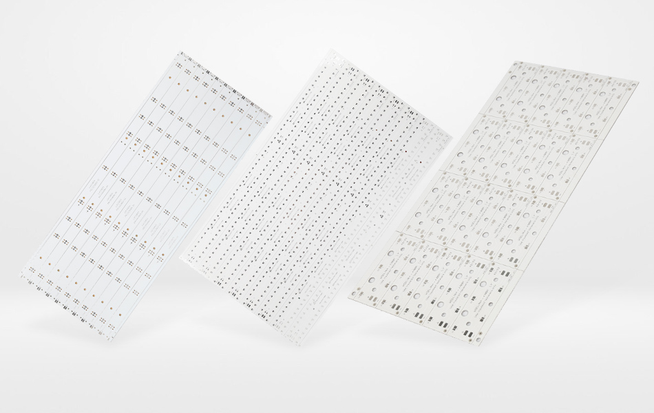
Sustainability and Circular Economy in Aluminum PCB Lifecycles
Eco-Friendly Manufacturing Practices
Aluminum PCB production is embracing sustainability:
Closed-Loop Aluminum Recycling: In-house recycling facilities recover and reprocess aluminum from production scrap, maintaining 95% of the original material’s thermal conductivity while reducing raw material consumption.
Renewable Energy-Powered Production: Solar and wind energy integration in manufacturing facilities cuts carbon emissions by 40% compared to traditional production methods.
Waterless Processing: Plasma etching and dry film photolithography eliminate hazardous wastewater in copper patterning, aligning with EU REACH and U.S. EPA environmental standards.
End-of-Life Management and Recycling
Innovative recycling approaches extend aluminum PCB value:
Selective Delamination: Thermal and chemical processes separate aluminum cores from copper and dielectric layers, enabling 90% material recovery for reuse in new PCB production.
Copper Recovery via Bioleaching: Bacteria-based extraction methods recover copper from end-of-life PCBs with 95% purity, reducing energy use by 70% compared to traditional smelting.
Repurposed Aluminum Cores: Refurbished aluminum substrates find second-life applications in low-power electronics, reducing e-waste in consumer devices.

Future Trends Shaping Aluminum PCB Technology
Smart and Adaptive Aluminum PCBs
Next-generation aluminum PCBs will feature integrated intelligence:
Self-Monitoring Layers: Embedded micro-sensors in aluminum cores detect temperature spikes, vibration levels, and material degradation, enabling predictive maintenance in critical infrastructure like power grids and healthcare equipment.
Thermally Reconfigurable Circuits: Phase-change materials in aluminum PCBs adjust conductivity based on operating conditions, optimizing performance across varying power loads in renewable energy inverters.
Material Convergence and Multi-Functionality
Aluminum PCBs are integrating diverse functionalities:
Energy Harvesting Integration: Thermoelectric modules embedded in aluminum cores convert waste heat into electricity, powering low-energy sensors in industrial machinery and smart buildings.
Structural-Electrical Integration: Aluminum PCBs that double as structural components reduce system weight in drones and electric aircraft, combining mechanical support with circuit functionality.
Global Standardization and Regulatory Alignment
Industry collaboration is driving consistency:
Cross-Industry Performance Standards: Unified testing protocols for thermal conductivity, vibration resistance, and environmental durability simplify material selection across automotive, aerospace, and consumer electronics sectors.
Sustainability Certification Frameworks: New standards for aluminum PCB recyclability and carbon footprint labeling enable transparent environmental claims, supporting global green initiatives.
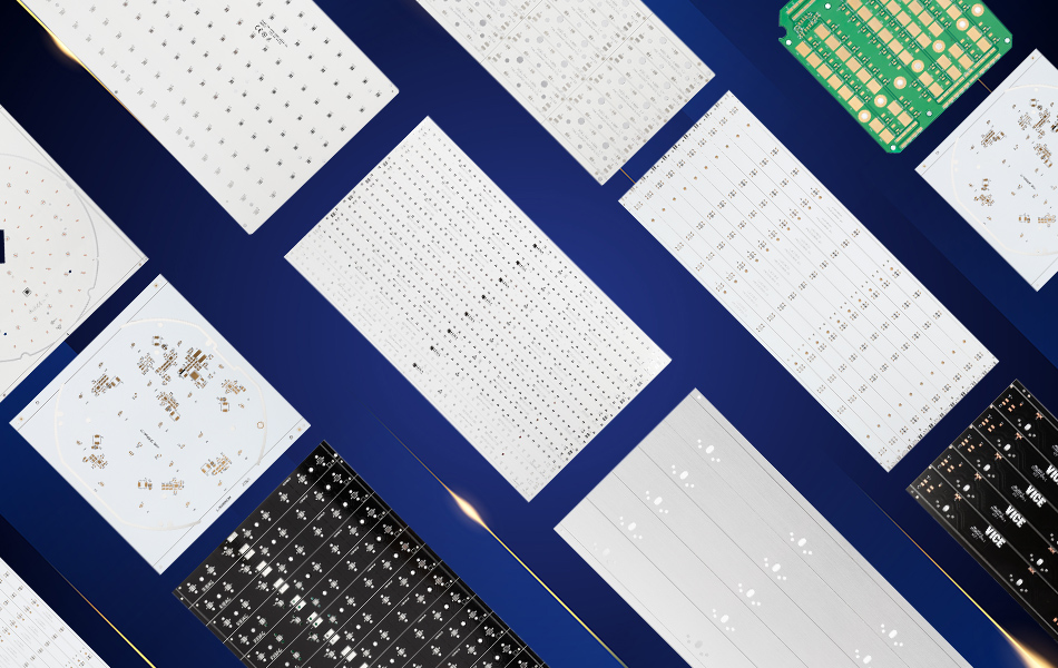
Conclusion: Aluminum PCBs as Enablers of Next-Generation Electronics
Aluminum PCBs have transcended their traditional role as thermal management solutions to become multi-functional platforms that drive innovation across industries. Through material science advancements, AI-driven design optimization, and a focus on sustainability, these PCBs are enabling technologies from quantum computing to green hydrogen energy systems. As electronic devices continue to evolve toward higher performance and lower environmental impact, aluminum PCBs will remain critical enablers—balancing thermal efficiency, electrical performance, and sustainability to power the next wave of technological advancement. For engineers and manufacturers, embracing aluminum PCB innovation is not just a technical choice but a strategic investment in the future of electronics.
In the fast-paced evolution of electronic engineering, aluminum printed circuit boards (PCBs) have emerged as a transformative technology, offering a unique combination of thermal efficiency, mechanical robustness, and design versatility. These PCBs leverage the inherent properties of aluminum to address the critical challenges of heat management, compact form factors, and reliable operation in diverse environments, making them indispensable across industries from lighting to aerospace. This article provides a comprehensive overview of aluminum PCBs, exploring their material science, design principles, manufacturing processes, industrial applications, and emerging trends, while highlighting their role in enabling the next generation of high-performance electronics.
The Foundation of Aluminum PCBs: Material Science
Aluminum Substrate: A Multifunctional Core
The aluminum substrate lies at the heart of these PCBs, serving as a foundational layer with distinct advantages:
Exceptional Thermal Conductivity: Aluminum’s high thermal conductivity allows for rapid dissipation of heat generated by power-hungry components, preventing thermal stress and ensuring stable operation. This is particularly crucial for devices where overheating could lead to performance degradation or component failure.
Mechanical Resilience: Aluminum alloys offer a favorable strength-to-weight ratio, making them resistant to bending, vibrations, and shocks. This mechanical durability is essential for applications in harsh environments, such as automotive, industrial, and aerospace systems.
Cost-Effective Formability: Aluminum’s malleability enables the creation of complex shapes and thin profiles, accommodating the compact designs demanded by modern electronics while maintaining structural integrity.
Dielectric Layers: Balancing Insulation and Heat Transfer
The dielectric layer in aluminum PCBs plays a dual role, separating the aluminum substrate from copper conductive layers while facilitating heat transfer:
Electrical Insulation: Ensures no short circuits between the aluminum core and copper traces, maintaining the integrity of electrical signals.
Thermal Interface: High-quality dielectric materials, such as ceramic-filled epoxies or polyimides, enhance heat transfer from components to the aluminum substrate, optimizing thermal management without compromising electrical performance.
Copper Layers: Conductive Pathways for Signal and Power
Copper, with its low electrical resistance, forms the conductive layers of aluminum PCBs:
Signal Traces: Designed to carry low-current signals with minimal loss, critical for high-frequency applications such as wireless communication and sensor networks.
Power Traces: Thicker copper foils are used for power distribution, reducing resistance and heat generation in high-current paths, the crucial in power electronics and motor control systems.
Design Principles for Aluminum PCBs
Thermal Management: The Critical Design Focus
Effective heat dissipation is the cornerstone of aluminum PCB design, involving strategic component placement and thermal pathway optimization:
Component Placement: Heat-generating components like power transistors, LEDs, and microprocessors are positioned to maximize contact with the aluminum substrate, allowing direct heat transfer. Thermal vias, which connect copper layers to the aluminum core, are strategically placed to create efficient heat dissipation paths.
Heat Sink Integration: The aluminum substrate can act as a natural heat sink, or it can be paired with external heat sinks for enhanced cooling. This is particularly important in high-power applications where maintaining optimal component temperatures is essential for longevity and performance.
Electrical Design: Signal Integrity and Power Efficiency
Trace Routing: High-speed signals are routed to minimize interference, with controlled impedance traces ensuring signal integrity in applications such as high-frequency data transmission. Power traces are designed to handle current loads efficiently, reducing voltage drops and energy loss.
Ground Plane Design: A solid ground plane on one or both sides of the PCB provides a stable reference for signals, reducing electromagnetic interference (EMI) and improving noise immunity in mixed-signal circuits.
Mechanical Design: Durability and Form Factor
Substrate Thickness: Tailored to application needs, with thinner substrates enabling compact, lightweight designs for portable devices and thicker substrates providing enhanced heat capacity for industrial power modules.
Mounting Solutions: Reinforced mounting holes and mechanical fixtures ensure the PCB remains secure in vibration-prone environments, while conformal coatings protect against moisture, dust, and chemical contaminants in harsh operating conditions.

Manufacturing Processes for Aluminum PCBs
Substrate Preparation
Material Cutting: Aluminum substrates are precision-cut using CNC milling or laser cutting to exact dimensions, followed by surface treatments to enhance the adhesion of dielectric layers and improve corrosion resistance.
Surface Treatment: Processes such as degreasing and micro-etching prepare the aluminum surface for lamination, ensuring a strong bond with dielectric materials and optimal thermal conductivity.
Layer Lamination
Dielectric Bonding: High-pressure lamination processes bond dielectric layers to the aluminum substrate, creating a stable base for copper layers. This step is critical for maintaining thermal and electrical performance, with automated presses controlling temperature and pressure to ensure uniform bonding.
Copper Layer Fabrication
Foil Lamination: Electrolytic copper foil is laminated to the dielectric layers, followed by photolithography or laser direct imaging (LDI) to transfer circuit patterns. LDI is particularly useful for fine-pitch traces in high-density designs, ensuring precise feature sizes and spacing.
Chemical Etching: Unwanted copper is removed using chemical etching, with post-etch inspection via automated optical inspection (AOI) to ensure trace integrity and eliminate defects.
Surface Finishing
Protective Coatings: Surface finishes such as electroless nickel immersion gold (ENIG), organic solderability preservative (OSP), or hot air solder leveling (HASL) are applied to copper traces to enhance solderability and corrosion resistance, depending on the application’s requirements.
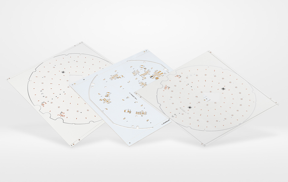
Industrial Applications of Aluminum PCBs
LED Lighting Systems
Commercial and Residential Lighting: Aluminum PCBs are widely used in LED panels, downlights, and linear fixtures, efficiently dissipating heat from LED arrays to maintain consistent light output and extend lifespan. Their formability allows for custom shapes in architectural lighting, while their thermal efficiency is crucial for high-brightness applications.
Automotive Lighting: In headlamps, taillights, and interior lighting, aluminum PCBs enable compact designs with reliable heat management, even in the temperature-sensitive environment of vehicle interiors.
Power Electronics
Power Supplies and Inverters: Aluminum PCBs handle the high currents and heat generated by power semiconductors in inverters for renewable energy systems and DC-DC converters, ensuring efficient power conversion and stable operation.
Battery Management Systems (BMS): Used in electric vehicles and energy storage systems to monitor and control battery cells, with thermal management critical to preventing thermal runaway and ensuring safety.
Automotive Electronics
Engine Control Units (ECUs): Operate reliably in the harsh environment of engine bays, with aluminum’s thermal and mechanical properties resisting high temperatures, vibrations, and moisture.
Advanced Driver-Assistance Systems (ADAS): Support high-speed data processing and sensor integration in ADAS modules, with aluminum PCBs enabling compact layouts and efficient heat dissipation from image processors and radar components.
Consumer Electronics
Portable Devices: Laptops, tablets, and gaming consoles use aluminum PCBs to manage heat from high-performance processors, enabling slim designs without compromising performance.
Wearable Technology: Smartwatches and fitness trackers rely on lightweight aluminum PCBs to integrate sensors, batteries, and wireless modules in compact form factors, balancing thermal efficiency with comfortable wear.
Industrial Control and Automation
Motor Drives and Robotics: Aluminum PCBs withstand the vibrations and high temperatures of industrial environments, supporting reliable operation of motor control circuits and robotic controllers.
Process Control Systems: Used in sensors and control panels for real-time monitoring in manufacturing plants, with conformal coatings protecting against dust and moisture.
Aerospace and Defense
Avionics Systems: Critical for navigation and communication modules in aircraft, where aluminum PCBs provide lightweight, high-reliability solutions that can withstand extreme temperatures and mechanical stress.
Military Electronics: Used in ruggedized devices such as portable radios and missile systems, combining thermal stability with resistance to shock and vibration.

Emerging Trends in Aluminum PCB Technology
Miniaturization and High-Density Integration
Microvia Technology: Laser-drilled microvias and fine-pitch traces enable high-density interconnects in compact devices such as IoT sensors and 5G modules, where every millimeter of board space is valuable.
3D Packaging: Aluminum PCBs facilitate vertical integration of components, creating 3D systems with enhanced thermal and electrical performance, ideal for advanced mobile devices and embedded systems.
Sustainable Manufacturing Practices
Eco-Friendly Materials: The industry is moving towards recycled aluminum substrates and water-based dielectric adhesives, reducing the environmental footprint while maintaining performance.
Energy-Efficient Processes: Low-temperature lamination and lead-free surface finishes align with global sustainability goals, ensuring aluminum PCBs are produced with minimal environmental impact.
Advanced Thermal Solutions
Hybrid Substrates: Composite materials combining aluminum with high-thermal-conductivity layers such as graphite or carbon fiber enhance heat dissipation, enabling higher power densities in applications like 5G power amplifiers and high-performance computing.
Phase-Change Materials (PCM): Integration of PCMs with aluminum PCBs provides passive thermal regulation, absorbing and releasing heat to maintain component temperatures within tight ranges in extreme environments.
Automation and Digital Design Tools
AI-Powered Design: Machine learning algorithms optimize component placement and thermal via routing, reducing design time and improving thermal performance in complex layouts.
Robotic Assembly: High-precision robotic systems ensure accurate component placement and soldering, improving yield in high-volume production and enabling micro-pitch applications.

Conclusion
Aluminum PCBs have revolutionized the electronics industry by offering a robust solution to the challenges of heat management, mechanical durability, and design flexibility. Their ability to support a wide range of applications, from everyday consumer devices to critical aerospace systems, highlights their versatility and importance in modern electronics. As technology continues to advance towards miniaturization, sustainability, and higher power densities, aluminum PCBs will evolve through material innovation, advanced manufacturing techniques, and 智能化 design tools. For engineers and designers, leveraging the unique advantages of aluminum PCBs is essential for creating reliable, efficient, and future-ready electronic systems that meet the demands of an increasingly connected and performance-driven world. By combining the natural strengths of aluminum with cutting-edge engineering, these PCBs are set to remain a cornerstone of high-performance electronics for years to come.
In the rapidly evolving landscape of electronic design, prototyping plays a critical role in transforming conceptual ideas into functional solutions. Among the diverse range of printed circuit board (PCB) technologies, 2 layer aluminum PCBs have emerged as a preferred choice for prototyping applications that demand a balance of thermal efficiency, mechanical robustness, and cost - effectiveness. This article explores the engineering principles, design considerations, manufacturing processes, and real - world applications of 2 layer aluminum PCB prototypes, providing insights into their role in modern electronic development.
Fundamentals of 2 Layer Aluminum PCBs
Structural Overview
A 2 layer aluminum PCB prototype consists of two primary conductive layers—top and bottom—separated by a dielectric layer bonded to an aluminum substrate. The aluminum base serves as both a mechanical support and a thermal dissipater, while the two copper layers handle signal transmission and power distribution. This simple yet effective structure makes it ideal for applications where moderate complexity and efficient heat management are required without the added cost and complexity of multi - layer designs.
The aluminum substrate, typically composed of alloys like 6xxx series, offers a combination of high thermal conductivity and mechanical strength. The dielectric layer, often a ceramic - filled epoxy or polyimide, provides electrical insulation while facilitating heat transfer from the copper traces to the aluminum base. This dual - layer configuration strikes a balance between performance and simplicity, making it a versatile choice for prototyping across industries.
Key Advantages for Prototyping
Thermal Efficiency: The aluminum substrate efficiently dissipates heat generated by components, preventing thermal stress that could compromise prototype functionality during testing. This is particularly important for power - intensive components like LEDs, voltage regulators, or microprocessors.
Cost - Effectiveness: Compared to multi - layer PCBs, 2 layer designs reduce material and manufacturing costs, making them suitable for initial design iterations where budget and time are critical.
Design Flexibility: The two - layer layout allows for straightforward component placement and trace routing, enabling rapid design modifications during the prototyping phase.
Mechanical Durability: The aluminum substrate provides robust mechanical support, resisting bending and vibrations, which is essential for prototypes tested in real - world environments.
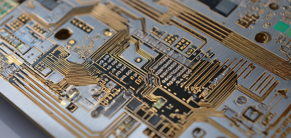
Design Considerations for 2 Layer Aluminum PCB Prototypes
Thermal Management Strategies
Component Placement
In 2 layer aluminum PCB prototypes, heat - generating components should be positioned on the top layer, directly above the aluminum substrate, to maximize heat transfer. Thermal vias—through - holes connecting the top copper layer to the aluminum base—are strategically placed around these components to create direct thermal pathways. The density and size of vias are optimized based on the component's power dissipation, with larger or more numerous vias used for higher - power devices.
Heat Sink Integration
For applications requiring enhanced thermal performance, the bottom layer of the PCB can be used to mount heat sinks or thermal pads. The aluminum substrate acts as a natural heat spreader, distributing heat across the board and into the heat sink, which is particularly effective in prototyping high - power LED fixtures or small - scale power supplies.
Electrical Design Principles
Trace Routing
In a 2 layer design, the top layer is typically used for signal traces and components, while the bottom layer serves as a ground plane or power distribution layer. This separation reduces electromagnetic interference (EMI) and provides a stable reference for signal integrity. High - speed signals should be routed on the top layer with controlled impedance, while the bottom layer's solid ground plane helps minimize noise.
Power Distribution
Power traces on the top layer are designed with sufficient width to handle the required current, avoiding voltage drops and excessive heating. The bottom layer can be used for distributing ground signals or low - voltage power, creating a balanced power - ground plane that improves overall circuit stability.
Mechanical Design Factors
Substrate Thickness
The thickness of the aluminum substrate is chosen based on the prototype's mechanical and thermal requirements. A thicker substrate offers greater mechanical strength and heat capacity, while a thinner substrate allows for more compact designs, suitable for portable or space - constrained applications.
Mounting and Form Factor
Mounting holes are incorporated into the design to secure the prototype within enclosures or test fixtures. The form factor—size and shape of the PCB—is optimized for the target application, with considerations for edge clearance, component spacing, and compatibility with mechanical interfaces.
Dielectric Layer Selection
Ceramic - filled epoxies are often preferred for dielectric layers in 2 layer prototypes due to their cost - effectiveness and balanced thermal - electrical properties. They offer better thermal conductivity than traditional FR4 dielectrics, ensuring efficient heat transfer to the aluminum substrate while providing adequate electrical insulation for most prototyping needs. Polyimide dielectrics may be used for high - temperature prototypes, such as those tested in industrial or automotive environments.

Manufacturing Processes for 2 Layer Aluminum PCB Prototypes
Design and Layout
CAD Tools
Designers use specialized software like Altium Designer, KiCad, or Eagle to create 2 layer layouts, ensuring proper component placement, trace routing, and thermal via positioning. These tools allow for thermal simulation to predict heat distribution and make iterative design improvements before manufacturing.
Gerber File Preparation
Gerber files, containing detailed layer information, are generated and verified for accuracy. Special attention is paid to thermal via placement and pad shapes to ensure proper heat dissipation and component soldering.
Material Preparation
Aluminum Substrate Cutting
The aluminum substrate is cut to the specified dimensions using CNC milling or laser cutting, ensuring precise edges and hole placement. The surface is cleaned and prepared to ensure proper adhesion of the dielectric layer and copper foil.
Dielectric Layer Lamination
A pre - cured dielectric sheet, either a ceramic - filled epoxy or polyimide, is laminated to the aluminum substrate using high - pressure and temperature processes. This creates a stable base for the copper layers, ensuring uniform thickness and thermal conductivity.
Copper Layer Fabrication
Copper Foil Lamination
Copper foil is laminated to both sides of the dielectric - coated aluminum substrate. The foil thickness is selected based on current requirements, with thicker foil used for power - intensive prototypes.
Photolithography and Etching
Photolithography is used to transfer the circuit design onto the copper foil. The exposed copper is etched away using chemical solutions, leaving the desired trace patterns on both the top and bottom layers. This process requires precision to ensure accurate trace widths and spacing, especially for fine - pitch components.
Via and Hole Formation
Drilling and Plating
Thermal vias and mounting holes are drilled using mechanical or laser drilling. Mechanical drilling is suitable for larger holes, while laser drilling offers precision for small vias. After drilling, the holes are plated with copper to ensure electrical connectivity between the top and bottom layers, with special attention to thermal vias to maximize heat transfer.
Surface Finishing
Options for Prototyping
Organic Solderability Preservative (OSP): A cost - effective option for prototyping, providing a thin organic layer that protects copper from oxidation and ensures good solderability.
Electroless Nickel Immersion Gold (ENIG): Used for prototypes requiring high - reliability connections, such as those with fine - pitch components or exposed contacts.
Hot Air Solder Leveling (HASL): A traditional finish suitable for prototypes where cost and ease of soldering are priorities.
Prototyping-Specific Considerations
Rapid prototyping services often use accelerated manufacturing processes, such as:
Laser Direct Imaging (LDI): For faster and more accurate pattern transfer, reducing lead times for small - batch prototypes.
Quick - Turn Lamination: Specialized presses that cure dielectric layers in shorter cycles, ideal for urgent prototype orders.

Quality Assurance for 2 Layer Aluminum PCB Prototypes
Electrical Testing
Continuity and Shorts
Using automated test equipment (ATE) or manual multimeters, engineers verify that there are no open circuits or short circuits between layers or traces. This is critical for ensuring the prototype's basic functionality before component assembly.
Impedance Matching
For high - speed signals, impedance testing ensures that trace widths and dielectric thicknesses match the designed impedance values, minimizing signal reflections and distortion.
hermal Testing
Infrared Thermography
Infrared cameras are used to map temperature distribution on the prototype when powered, identifying hotspots and verifying the effectiveness of thermal vias and component placement. This helps engineers optimize the design for better heat dissipation in subsequent iterations.
Thermal Cycling
Prototypes are subjected to repeated temperature cycles (e.g., -40°C to +85°C) to test the durability of the aluminum substrate, dielectric layer, and solder joints, ensuring they can withstand operational temperature fluctuations.
Mechanical Testing
Bend and Vibration Tests
Mechanical tests evaluate the substrate's resistance to bending and vibrations, ensuring the prototype remains intact during handling and real - world use. This is particularly important for portable or automotive prototypes.
Mounting Stability
Testing the integrity of mounting holes and fixtures ensures the prototype can be securely installed in enclosures or test setups without mechanical failure.
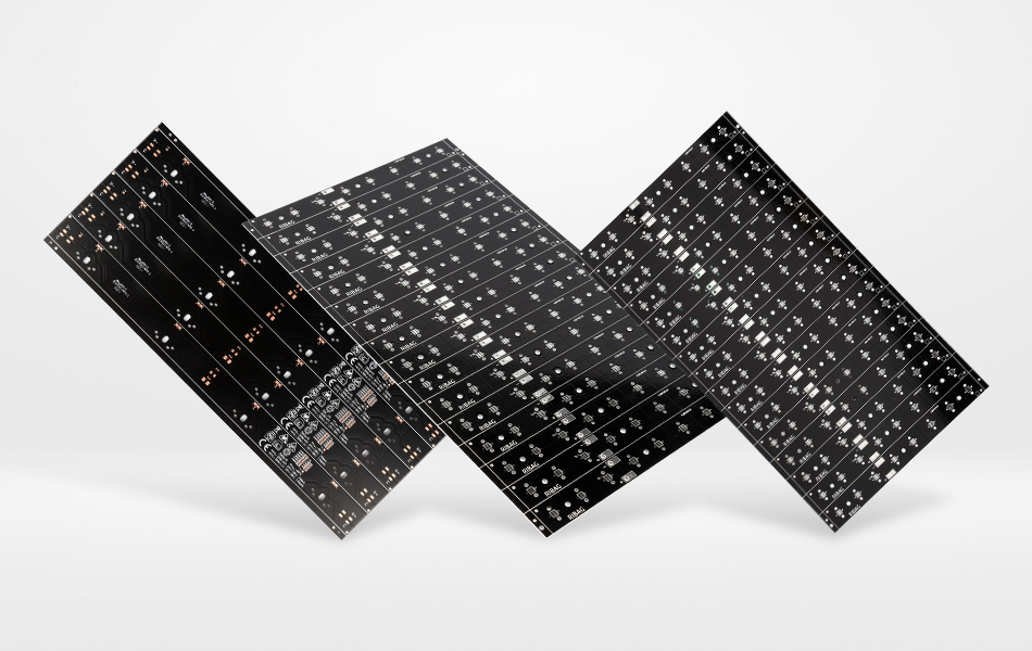
Applications of 2 Layer Aluminum PCB Prototypes
LED Lighting Prototyping
Commercial and Residential Fixtures
Prototypes for LED panels, downlights, or linear fixtures use 2 layer aluminum PCBs to manage heat from LED arrays. The two - layer design allows for straightforward placement of LEDs on the top layer, with the bottom layer serving as a heat sink interface, ensuring uniform light output and extended LED lifespan during testing.
Automotive Lighting
Prototypes for automotive taillights, headlights, or interior lighting leverage the aluminum substrate's vibration resistance and thermal efficiency. The two - layer layout simplifies the integration of LED drivers and thermal management components, critical for meeting automotive reliability standards.
Power Electronics Prototyping
DC - DC Converters
Prototypes for small - to - medium - power DC - DC converters use 2 layer aluminum PCBs to dissipate heat from power transistors and inductors. The bottom layer's ground plane provides a stable reference for high - frequency signals, while the aluminum substrate prevents overheating during load testing.
Battery Management Systems (BMS)
BMS prototypes for electric vehicles or energy storage systems rely on 2 layer aluminum PCBs to manage heat from battery monitoring circuits and power switches, ensuring safe and efficient operation during prototype validation.
Consumer Electronics Prototyping
Portable Devices
Prototypes for laptops, tablets, or wearable devices use 2 layer aluminum PCBs to balance thermal management and compact design. The aluminum substrate helps dissipate heat from processors or batteries, while the two - layer layout allows for efficient routing of high - speed data signals and power traces.
Audio Equipment
Audio amplifiers or soundbars use 2 layer aluminum prototypes to manage heat from power amplifiers, ensuring stable operation and reducing noise interference through proper ground plane design.
Industrial and IoT Prototyping
Industrial Controllers
Prototypes for motor controllers or sensor hubs in industrial automation use 2 layer aluminum PCBs to withstand harsh environments. The aluminum substrate's corrosion resistance and thermal efficiency are critical for maintaining performance in dusty, humid, or high - temperature settings.
IoT Sensors
Compact IoT sensor prototypes benefit from the lightweight and thermal properties of 2 layer aluminum PCBs, ensuring reliable operation in remote or space - constrained locations, such as smart city sensors or environmental monitoring devices.

Market Trends and Future Directions
Growing Demand for Rapid Prototyping
The rise of small - batch manufacturing and customized electronics has increased the demand for 2 layer aluminum PCB prototypes. Companies are leveraging these prototypes to quickly validate designs, reduce time - to - market, and minimize risks associated with mass production.
Integration with Advanced Materials
Future prototypes may incorporate advanced dielectric materials with higher thermal conductivity, such as boron nitride nanocomposites, to further enhance heat dissipation in 2 layer designs. These materials could enable smaller form factors for high - power prototypes without compromising performance.
Sustainable Prototyping Practices
Environmental concerns are driving the adoption of recycled aluminum substrates and eco - friendly dielectric materials in prototyping. Manufacturers are also implementing greener etching and plating processes to reduce the environmental impact of 2 layer aluminum PCB production.
Automation in Prototyping
Advanced automation tools, such as AI - powered design assistants and robotic assembly systems, are streamlining the prototyping process. These technologies reduce human error, accelerate design iterations, and enable real - time thermal and electrical simulations for more accurate 2 layer aluminum PCB prototypes.
Conclusion
2 layer aluminum PCB prototypes serve as a vital bridge between conceptual design and mass production, offering a balanced combination of thermal efficiency, cost - effectiveness, and design flexibility. Their role in prototyping spans diverse industries, from LED lighting and power electronics to consumer devices and industrial automation, enabling engineers to validate designs in real - world scenarios. As technology continues to advance, the integration of advanced materials, sustainable practices, and automation will further enhance the capabilities of 2 layer aluminum PCBs, solidifying their position as a cornerstone of modern electronic prototyping. By understanding their engineering fundamentals and practical applications, designers and manufacturers can leverage these prototypes to drive innovation and bring reliable, high - performance products to market efficiently.
In the ever - evolving landscape of modern lighting technology, LED circuits boards have emerged as the linchpin for efficient and innovative illumination solutions. These boards serve as the foundation for powering light - emitting diodes (LEDs), enabling them to deliver superior performance, energy efficiency, and extended lifespan. From residential and commercial settings to specialized applications in automotive, aerospace, and healthcare, LED circuits boards have revolutionized the way we light our world. This article delves deep into the world of LED circuits boards, exploring their material composition, design principles, manufacturing processes, quality assurance measures, diverse applications, and emerging market trends.
Material Composition of LED Circuits Boards
Substrate Materials
The choice of substrate material in LED circuits boards is a critical decision that significantly impacts the overall performance and reliability of the lighting system. Different substrate materials offer distinct advantages, depending on the specific requirements of the application.
Aluminum substrates have gained widespread popularity due to their excellent thermal conductivity. LEDs generate a significant amount of heat during operation, and efficient heat dissipation is crucial for maintaining their performance and lifespan. Aluminum substrates effectively transfer heat away from the LEDs, preventing overheating and ensuring stable operation. Additionally, aluminum offers good mechanical strength and formability, making it suitable for a variety of lighting fixtures.
FR4, a fiberglass - reinforced epoxy laminate, is another commonly used substrate material. It provides good electrical insulation and mechanical stability, making it suitable for applications where cost - effectiveness and standard performance are required. However, FR4 has relatively lower thermal conductivity compared to aluminum, which may limit its use in high - power LED applications where efficient heat dissipation is essential.
Ceramic substrates, such as aluminum nitride (AlN) and aluminum oxide (Al₂O₃), offer superior thermal conductivity and electrical insulation properties. They are ideal for high - power, high - temperature applications where reliable performance and long - term durability are critical. Ceramic substrates can withstand extreme operating conditions, making them suitable for applications in automotive, aerospace, and industrial lighting.
Dielectric Layers
The dielectric layer in LED circuits boards serves as an electrical insulator between the conductive traces and the substrate, while also facilitating heat transfer. The selection of the dielectric material is crucial for optimizing the electrical and thermal performance of the board.
Polyimide - based dielectrics are known for their high - temperature resistance and excellent electrical insulation properties. They can withstand elevated temperatures without significant degradation, making them suitable for high - power LED applications. Polyimide dielectrics also offer low dielectric loss, which helps to minimize signal attenuation and improve the overall efficiency of the circuit.
Ceramic - filled epoxies are another popular choice for dielectric layers. These materials combine the advantages of epoxy resins, such as good adhesion and processability, with the high thermal conductivity of ceramic fillers. Ceramic - filled epoxies provide a cost - effective solution for improving the thermal performance of LED circuits boards, making them suitable for a wide range of applications.
Conductive Traces
Copper is the most commonly used material for the conductive traces in LED circuits boards due to its low electrical resistance and excellent conductivity. The thickness and width of the copper traces are carefully designed to ensure efficient power delivery to the LEDs while minimizing power losses and heat generation.
In high - power LED applications, thicker copper traces are often used to handle the increased current flow. This helps to reduce voltage drops and ensure that each LED receives the appropriate amount of power. Surface treatments, such as electroless nickel immersion gold (ENIG), electroless nickel electroless palladium immersion gold (ENEPIG), and organic solderability preservatives (OSP), are applied to the copper traces to enhance their corrosion resistance, solderability, and long - term reliability.
Design Principles of LED Circuits Boards
Thermal Management Design
Thermal management is one of the most critical aspects of LED circuits board design. Effective heat dissipation is essential for maintaining the performance and lifespan of the LEDs, as well as ensuring the overall reliability of the lighting system.
Thermal vias play a crucial role in thermal management by providing a direct pathway for heat to transfer from the LEDs to the substrate. These vias are strategically placed to maximize heat dissipation and minimize thermal resistance. The size, number, and distribution of thermal vias are carefully optimized based on the power requirements and thermal characteristics of the LEDs.
In addition to thermal vias, heat sinks and heat spreaders are often used to enhance heat dissipation. Heat sinks increase the surface area available for heat transfer, while heat spreaders help to evenly distribute the heat across the substrate. The design of the heat sink and heat spreader is optimized to ensure efficient heat transfer and minimize the temperature gradient across the LED array.
Electrical Design
The electrical design of LED circuits boards focuses on ensuring stable and efficient power supply to the LEDs. This includes designing the appropriate current - limiting circuits, voltage regulators, and driver circuits to regulate the current and voltage supplied to the LEDs.
In multi - LED arrays, careful consideration must be given to the electrical configuration of the LEDs, whether in series, parallel, or a combination of both. Series - connected LEDs require a higher voltage but lower current, while parallel - connected LEDs require a lower voltage but higher current. The choice of electrical configuration depends on the specific requirements of the application, such as the desired brightness, color temperature, and power consumption.
Electromagnetic compatibility (EMC) is also an important consideration in the electrical design of LED circuits boards. LED drivers can generate electromagnetic interference (EMI), which may disrupt other electronic devices in the vicinity. Therefore, proper shielding, filtering, and layout techniques are employed to minimize EMI and ensure compliance with EMC standards.
Mechanical Design
The mechanical design of LED circuits boards takes into account factors such as the physical dimensions of the board, the mounting method, and the mechanical stresses it may encounter during operation. The size and shape of the board are determined by the requirements of the lighting fixture and the number and arrangement of the LEDs.
Mounting holes and attachment mechanisms are incorporated into the board design to securely fasten the board to the lighting fixture. The choice of mounting method, such as screw - mounting, snap - fitting, or adhesive bonding, depends on the design of the fixture and the environmental conditions in which the board will operate.
In outdoor or harsh - environment applications, the mechanical design of the board must also consider factors such as resistance to vibration, shock, and corrosion. Reinforcement features, such as stiffeners or protective enclosures, may be added to enhance the mechanical durability of the board.
Optical Design
Optical design is closely intertwined with the electrical and mechanical design of LED circuits boards. The placement and orientation of the LEDs on the board directly affect the light distribution pattern of the lighting fixture. Therefore, careful consideration must be given to the optical design to ensure that the desired light output characteristics are achieved.
Optical components, such as lenses, reflectors, and diffusers, are often used in conjunction with LED circuits boards to control the light distribution and enhance the performance of the lighting system. The design of these optical components is optimized to maximize the light extraction efficiency and minimize light losses.

Manufacturing Processes of LED Circuits Boards
Circuit Board Fabrication
The fabrication of LED circuits boards involves a series of processes, including drilling, plating, lamination, and etching. These processes are carefully controlled to ensure the precision and quality of the board.
Drilling is the first step in the fabrication process, which creates holes for vias, component mounting, and other purposes. Mechanical drilling and laser drilling are the two commonly used methods for drilling holes in circuit boards. Mechanical drilling is a cost - effective method for creating larger holes, while laser drilling offers higher precision and is suitable for creating smaller holes.
Plating is used to deposit a layer of copper on the drilled holes and the surface of the board to ensure electrical conductivity. Electroless plating and electrolytic plating are the two main types of plating processes used in circuit board fabrication. Electroless plating is used to deposit a thin layer of copper on non - conductive surfaces, while electrolytic plating is used to build up the copper layer to the desired thickness.
Lamination is the process of bonding the different layers of the circuit board together, including the substrate, dielectric layer, and copper traces. High - pressure lamination and vacuum lamination are the two commonly used methods for lamination. High - pressure lamination uses heat and pressure to bond the layers together, while vacuum lamination uses a vacuum to remove air bubbles and ensure a uniform bond.
Etching is the process of removing the unwanted copper from the surface of the board to create the desired circuit pattern. Chemical etching and dry etching are the two main types of etching processes used in circuit board fabrication. Chemical etching uses chemicals to dissolve the unwanted copper, while dry etching uses plasma or ion beams to remove the copper.
Component Mounting
After the circuit board is fabricated, the next step is to mount the components onto the board. Surface - mount technology (SMT) is the most commonly used method for mounting components on LED circuits boards. SMT involves placing the components onto the surface of the board using automated pick - and - place machines and then soldering them in place using reflow soldering or wave soldering.
Reflow soldering is the most widely used soldering method for SMT components. It involves heating the board in a reflow oven, which melts the solder paste and creates a strong electrical and mechanical connection between the components and the board. Wave soldering is another soldering method that is commonly used for through - hole components. It involves passing the board over a wave of molten solder, which solders the components in place.
Testing and Quality Assurance
Once the components are mounted on the board, the next step is to test the board to ensure that it meets the required specifications. Electrical testing, optical testing, and thermal testing are the three main types of tests that are performed on LED circuits boards.
Electrical testing involves testing the electrical properties of the board, such as the resistance, capacitance, and impedance of the components and the traces. Optical testing involves testing the light output characteristics of the board, such as the luminous intensity, color temperature, and color rendering index of the LEDs. Thermal testing involves testing the thermal performance of the board, such as the temperature distribution and the heat dissipation efficiency of the LEDs and the substrate.
In addition to these tests, quality assurance measures are also implemented throughout the manufacturing process to ensure the quality and reliability of the boards. These measures include incoming material inspection, in - process inspection, and final inspection.

Applications of LED Circuits Boards
Residential Lighting
LED circuits boards are widely used in residential lighting applications, such as ceiling lights, wall sconces, table lamps, and recessed downlights. The energy - efficiency and long lifespan of LEDs make them an attractive choice for homeowners, as they can significantly reduce energy consumption and maintenance costs.
LED circuits boards also offer a high degree of design flexibility, allowing for the creation of customized lighting solutions that can enhance the ambiance and functionality of any living space. With the ability to control the color, brightness, and intensity of the light, LED circuits boards can be used to create a variety of lighting effects, from warm and cozy to bright and vibrant.
Commercial Lighting
Commercial buildings, such as offices, shopping malls, hotels, and hospitals, also benefit greatly from the use of LED circuits boards. In large - scale commercial applications, the energy savings and reduced maintenance costs offered by LEDs can be substantial, making them a cost - effective lighting solution.
LED circuits boards can be used to create a variety of lighting designs for commercial spaces, including general illumination, task lighting, and accent lighting. They can also be integrated with smart lighting systems, allowing for the control and automation of the lighting based on occupancy, daylight levels, and other factors.
Outdoor Lighting
Outdoor lighting applications, such as streetlights, parking lot lights, landscape lighting, and floodlights, require robust and reliable lighting solutions that can withstand harsh environmental conditions. LED circuits boards are well - suited for outdoor use, as they offer high energy efficiency, long lifespan, and resistance to weather, vibration, and shock.
LED outdoor lighting can also be designed to meet specific lighting requirements, such as brightness, color temperature, and light distribution. With the use of advanced optical components, LED outdoor lighting can provide uniform and efficient illumination, while minimizing light pollution and energy waste.
Automotive Lighting
The automotive industry has witnessed a rapid adoption of LED technology in recent years, and LED circuits boards play a crucial role in this trend. LED headlights, taillights, interior lighting, and daytime running lights are all powered by LED circuits boards, offering improved visibility, energy efficiency, and design flexibility.
LED automotive lighting can also be integrated with advanced driver - assistance systems (ADAS), such as adaptive cruise control, lane departure warning, and automatic emergency braking. By providing precise and reliable lighting, LED circuits boards can enhance the safety and performance of modern vehicles.
Specialized Lighting Applications
LED circuits boards are also used in a variety of specialized lighting applications, such as horticultural lighting, medical lighting, and aviation lighting. In horticultural lighting, LEDs are used to provide the specific wavelengths of light required for plant growth, resulting in increased crop yields and improved plant quality.
In medical lighting, LEDs are used to provide high - quality, flicker - free illumination for surgical procedures, examination rooms, and other medical applications. LED medical lighting can also be designed to meet specific color temperature and color rendering requirements, ensuring accurate diagnosis and treatment.
In aviation lighting, LEDs are used to provide reliable and energy - efficient lighting for aircraft interiors and exteriors. LED aviation lighting can also be integrated with advanced lighting control systems, allowing for the adjustment of the lighting based on the flight phase, cabin conditions, and other factors.

Market Trends of LED Circuits Boards
Growing Demand for Energy - Efficient Lighting
The increasing focus on energy conservation and environmental sustainability is driving the demand for energy - efficient lighting solutions, such as LED circuits boards. Governments around the world are implementing strict energy - efficiency regulations and incentives to promote the adoption of LED lighting, which is expected to fuel the growth of the LED circuits board market in the coming years.
Advancements in LED Technology
The continuous advancements in LED technology, such as the development of high - power, high - efficiency LEDs and the improvement of LED packaging and thermal management, are also contributing to the growth of the LED circuits board market. These advancements are enabling the development of more powerful, efficient, and reliable LED lighting systems, which are expected to expand the application scope of LED circuits boards.
Integration of Smart Lighting Systems
The integration of LED circuits boards with smart lighting systems, such as wireless control, occupancy sensing, and daylight harvesting, is becoming increasingly popular. Smart lighting systems offer a range of benefits, such as energy savings, convenience, and enhanced user experience, which is expected to drive the demand for LED circuits boards in the smart home and commercial building markets.
Growing Demand for Miniaturization and High - Density Integration
The trend towards miniaturization and high - density integration in the electronics industry is also driving the demand for smaller, more compact LED circuits boards. As the size of the LEDs and other components continues to shrink, the design and manufacturing of LED circuits boards need to adapt to accommodate these changes, which is expected to create new opportunities for innovation and growth in the LED circuits board market.
In conclusion, LED circuits boards have become an essential component in the modern lighting industry, offering a wide range of benefits, such as energy efficiency, long lifespan, design flexibility, and reliability. As the demand for energy - efficient lighting solutions continues to grow, and the advancements in LED technology and smart lighting systems continue to evolve, the future of LED circuits boards looks promising. Manufacturers and designers of LED circuits boards need to stay updated with the latest trends and technologies to meet the changing needs of the market and drive the continued growth and innovation of the LED lighting industry.

Step 1: Get in Touch
Click “Skype” button、whatsapp 、info@xunruilyjm.zhu、calling us or sending us “Instant message” through “Request a quote”button,which is on the upper right corner, fill in the email and your message Then you will get an agent from Apollo to get in touch with you and get 50USD PCB coupons immediately.
Step 2: Gerber preview
Send us an email with all the data which is required for the PCB and then Your Agent will send to our engineers team who will preview and evaluate your gerber files and technical specifications,you will get an estimated quote price,the price is nearly 99.5% accurate but may undergo change when re-checking process have been done and found special requirement such as “Copper tended vias”,resign-plug vias,panelization changes etc.Although RS274-X format Gerber data is our standard manufacturing data, we also accept Gerber,PADs, and Eagle file and .PCB file . Please note we will convert your PADs files、.pcb files or Eagle file to Gerber data and then ask for your confirmation before proceeding towards PCB manufacturing line.
Step 3: Order review
After you confirmed orders, our engineer will review the order ASAP. If any issues were found, we will contact you by email or online chat. Please make sure the email address you filled on our website is valid.EQ(if have) and working files will be generated and sent to customers for approval before starting production.
Step 4: How to Pay.
Once the PCB order passes our audit and was confirmed, customers can choose the shipping method and make the payment by PayPal or choose any other available payment methods (We also accept bank transfer,Western union and so on. Please contact us at info@xunruilyjm.zhu for further details if you choose these payment methods). Before paying, please confirm the shipping information you have provided is correct and accurate; especially the address, city name and the corresponding post code.Specially Note:When making payment by bank transfer,please fill our full company name.
Step 5: PCB Fabrication.
The PCB fabrication job will be started immediately once the payment is received and EQ&Gerber files are approved. You can check the manufacture process from the production status provided by our Agent.
Step 6: Delivery:
Once the parcel is shipped out, the tracking number and PI/PL will be sent to you and we will keep you updated with shipping status until you received the goods successfully.
Please note the customs tax fee is different for different countries, before shipping you may consult with your local DHL company or customs office to check the detailed information. Please note the order will be declared as real value or customer requirement; let us know once you place your order (you can change the declared value once you make the payment). Note that all import duties will be on buyers’ account.
Finally, if you still have problem with the order process, please feel free to contact us through online chat、via email: info@xunruilyjm.zhu、by Skype: frank417276767 or call us at:086-755-29438407, we will respond to you as soon as possible within 24 hours. We hope to make our ordering procedure as simple and flexible as possible.
● How to re-order in Apollopcb?
A. Why do you need to re-order?
As we know, different engineers will deal with PCB file in different way so that some details of your new PCB orders will be different. If you want to order the same boards as the samples which you placed in Apollopcb and if you want to save toolings cost(OTC),you need to re-order it instead of placing new order so that your order will be dealt with by the same engineer that operated on your sample order and it will be same as the sample you have been provided with.
B. How to reorder in Apollo?
If you need to reorder the same boards, whose sample order is provided to you by Apollo, follow the steps listed below. Make sure there are no changes in design of your new order and it is same as your previous orders. First, you send emails to your agent and advise part number of your orders. Second, summit repeat orders.If you provided gerber files,our agent and engineers will do the qualifications again and advise if there is any changes on design.We will update the price if we have to setup new toolings due to design changes
PCB Assembly Process
Firstly, you need to send the PCB gerber file, BOM list, Pick and place file. Please note that Gerber,PADs, and Eagle file and .PCB file will be accepted by Apollopcb. If your PCB file is in some other format, please export the Gerber file to us for PCB fabrication. BOM list is a file that contains all components with part number, manufacturer number, specifications, quantity, packages, and legends etc.
We strongly recommend that we perform simple functional tests on your products before shipping them, so that we can guarantee 100% pass rate. We need customers to provide simple test guidelines, we manually or use test fixtures for testing to ensure compliance Shipment of electrical measurement values that meet your requirements.
Secondly, please send us the above mentioned files as mentioned above via email: info@xunruilyjm.zhu. The quotation will come out within 48-72 hours which depends on your components, the PCB complexity and difficulty degree.
● Files needed: Schematic (DSN or PowerLogic), netlist, package, structure chart (DXF), Components file, layout requirements etc.
● Layout and wiring judgment: according to the design standard, design instruction, customer's design requirements and related checklist.
● Layout check and confirm: provide layout file and structure file for customers to check if the layout makes sense and confirm the stack-up program, impedance program, structure and package, also confirm the trace specification.
● Layout file output: PCB original file, Gerber file, pick and place file, framed stencil file and structure file etc. If you have any PCB layout job to get done, don’t hesitate to contact us: info@xunruilyjm.zhu.

Got project ready to assembly? Contact us: info@apollopcb.com


We're not around but we still want to hear from you! Leave us a note:

Leave Message to APOLLOPCB
