-
- PCB TYPE
- PRINTED CIRCUIT BOARD PROTOTYPE ALUMINUM PRINTED CIRCUIT BOARD R&F PCB FPC HIGH FREQUENCY PCB HIGH-TG PCB HEAVY COPPER PCB HDI PCB PCB FOR LIGHTING METAL CORE PCB
time:Sep 12. 2025, 11:57:34
In the fast-evolving world of electronics, the demand for more compact, efficient, and powerful devices is higher than ever. To meet these demands, the design and manufacturing of electronic circuit boards have seen significant advancements. One such innovation is the use of blind and buried vias in high-density interconnect (HDI) PCBs. In this article, we will explore what blind and buried vias are, their advantages, and why choosing the right PCB manufacturer is crucial for your electronic projects.
Printed Circuit Boards (PCBs) are the backbone of any electronic device. They connect various components on the board using conductive pathways. In traditional PCBs, through-hole vias are used to connect different layers of the board. However, as devices become more compact, the need for more advanced techniques has led to the development of blind and buried vias.
Blind vias connect the outer layer of the PCB to one or more inner layers without going all the way through the board. This allows for more surface area on the outer layers for components and routing, making it ideal for compact designs.
Buried vias, on the other hand, are located entirely within the internal layers of the PCB. These vias do not reach the outer layers, allowing for even more compact and efficient designs by freeing up more space on the surface.

The use of blind and buried vias in PCBs offers numerous benefits, especially for high-density interconnect applications.
By using blind and buried vias, PCB designers can save a significant amount of space on the board. This is crucial for devices where space is at a premium, such as smartphones, tablets, and other portable electronics.
Signal integrity is a critical factor in electronic devices. Blind and buried vias help reduce the length of conductive pathways, which minimizes signal loss and improves the overall performance of the device.
With the ability to connect different layers without using through-holes, designers have more flexibility in routing and placing components. This leads to more innovative and efficient designs.

Selecting the right manufacturer for your PCB needs is crucial for ensuring quality, reliability, and performance. Here are some factors to consider when choosing a blind and buried vias PCB manufacturer:
Look for a manufacturer with extensive experience in producing high-density interconnect PCBs. Their expertise will ensure that your boards are manufactured to the highest standards and meet your specific requirements.
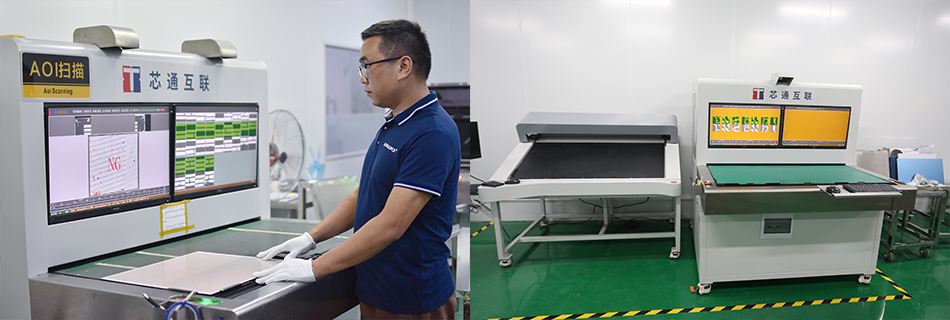
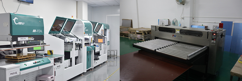
A reputable manufacturer should have state-of-the-art facilities and equipment to produce PCBs with blind and buried vias. This includes advanced drilling and plating technologies to ensure precision and quality.
Quality is paramount in PCB manufacturing. Ensure that the manufacturer follows strict quality control processes and complies with industry standards. Certifications such as ISO9001 and IPC-A-600 are indicators of a commitment to quality.
Each project may have unique requirements. A good manufacturer should offer customization options and provide technical support to help you achieve your design goals.

Blind and buried vias are used in a wide range of electronic applications. Here are some common areas where these advanced PCB technologies are applied:
Devices like smartphones, tablets, and laptops benefit from the compact and efficient design enabled by blind and buried vias. These vias allow for more components and functionality in a smaller footprint.
In the medical field, devices such as diagnostic equipment and wearable health monitors require high-density PCBs to function effectively. Blind and buried vias help achieve the necessary miniaturization and reliability.
Modern vehicles are equipped with numerous electronic systems, from infotainment to advanced driver-assistance systems (ADAS). Blind and buried vias contribute to the compact and robust design needed for automotive applications.
Telecommunications equipment, such as routers and switches, demands high performance and reliability. Using blind and buried vias in PCBs helps meet these requirements by optimizing signal integrity and space utilization.

The advancement of PCB technology with blind and buried vias has revolutionized the design and manufacturing of electronic circuit boards. These innovations enable more compact, efficient, and powerful electronic devices across various industries. When selecting a blind and buried vias PCB manufacturer, it's essential to choose a partner with the expertise, capabilities, and commitment to quality to ensure the success of your projects.
Whether you are developing consumer electronics, medical devices, automotive systems, or telecommunications equipment, the right PCB manufacturer can make all the difference in achieving your design goals and delivering high-performance products to the market.
By understanding the benefits and applications of blind and buried vias, you can make informed decisions for your next electronic project and stay ahead in the competitive world of technology.

Got project ready to assembly? Contact us: info@apollopcb.com


We're not around but we still want to hear from you! Leave us a note:

Leave Message to APOLLOPCB
