-
- PCB TYPE
- PRINTED CIRCUIT BOARD PROTOTYPE ALUMINUM PRINTED CIRCUIT BOARD R&F PCB FPC HIGH FREQUENCY PCB HIGH-TG PCB HEAVY COPPER PCB HDI PCB PCB FOR LIGHTING METAL CORE PCB
time:Aug 13. 2025, 10:50:35
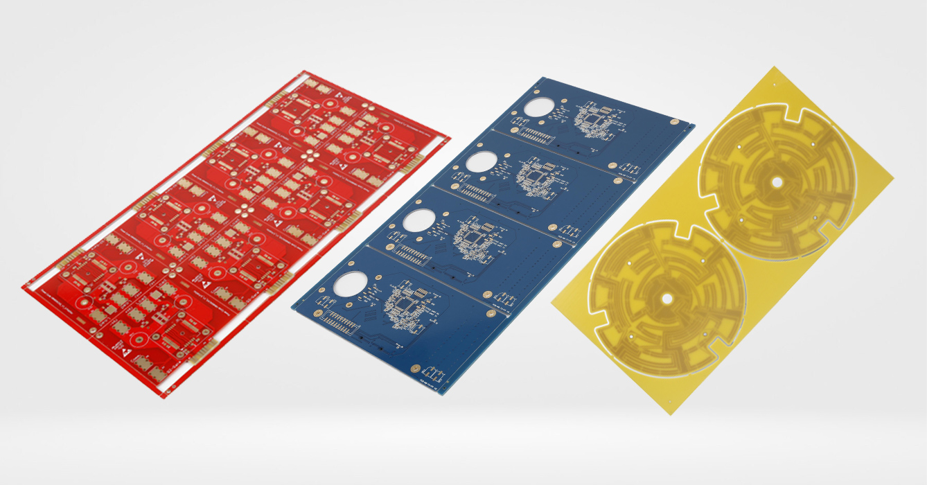
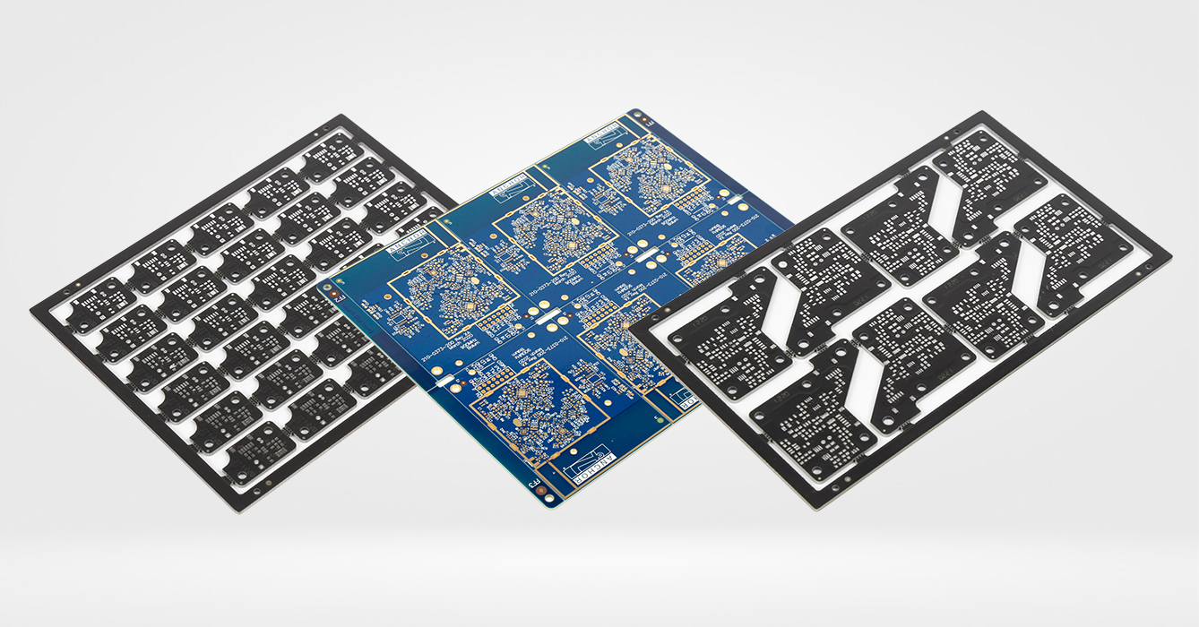
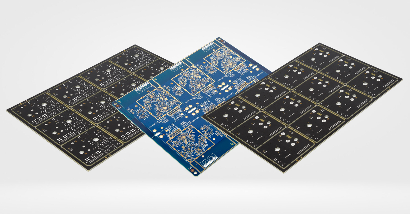
In the realm of printed circuit boards, the 4 Layer Rigid FR4 Circuit Board stands as a versatile solution, bridging the gap between simple 2-layer designs and more complex multi-layer configurations. Combining the mechanical stability of rigid FR4 with the functional benefits of four conductive layers, this type of circuit board has become a staple in modern electronics, offering enhanced routing flexibility, improved signal integrity, and efficient power distribution. Unlike single or 2-layer boards, which are limited by space and functionality, 4 layer rigid FR4 circuit boards accommodate denser components and more intricate circuits without sacrificing reliability. This article delves into the unique characteristics, design principles, manufacturing processes, and applications of 4 layer rigid FR4 circuit boards, highlighting their role in enabling compact, high-performance electronic devices.
A 4 Layer Rigid FR4 Circuit Board consists of four conductive copper layers separated by insulating FR4 substrate layers, bonded together through a lamination process. This structure is designed to maximize functionality within a compact form factor, making it ideal for devices where space is limited but performance requirements are high.
The layers are typically arranged in a symmetrical stackup to minimize warping during manufacturing and operation. A common configuration includes:
Two outer layers (top and bottom) dedicated to component mounting and signal routing.
Two inner layers often used for power distribution and ground planes, which help reduce electromagnetic interference (EMI) and improve signal integrity.
FR4, the core material, is chosen for its excellent electrical insulation, mechanical rigidity, and cost-effectiveness. Its glass fiber-reinforced epoxy composition provides stability across temperature variations and mechanical stress, ensuring the board maintains its shape and performance in diverse environments—from consumer electronics to industrial machinery.
Compared to 2-layer boards, 4 layer designs offer greater routing density, allowing engineers to incorporate more components and complex circuits without increasing the board’s physical size. This makes them a popular choice for devices that require a balance of functionality, size, and cost.

The 4 layer configuration offers several key advantages over simpler designs, making it a preferred option for mid-to-high complexity electronics:
With four conductive layers, designers have more space to route traces, reducing the need for complex crossover patterns or excessive vias (holes connecting layers). This flexibility is critical for accommodating high-density components like microprocessors, sensors, and memory chips, which require numerous connections. The inner layers can be dedicated to power and ground, freeing the outer layers for signal traces, minimizing interference, and simplifying routing.
Signal integrity—maintaining the quality of electrical signals as they travel through the board—is significantly enhanced in 4 layer designs. The inner ground plane acts as a shield, reducing EMI and crosstalk (unwanted signal interference between adjacent traces). This is especially important for high-frequency signals, such as those in communication devices or data processing systems, where signal degradation can lead to performance issues or errors.
4 layer boards often dedicate one or more inner layers to power distribution, creating a low-resistance path for current flow. This “power plane” ensures stable voltage delivery to components, reducing voltage drops and noise that can disrupt sensitive electronics. Compared to 2-layer boards, which rely on discrete power traces, 4 layer designs distribute power more evenly, improving overall system reliability.
The symmetrical stackup of 4 layer rigid FR4 circuit boards minimizes warping caused by thermal expansion and contraction. The FR4 substrate’s inherent rigidity, combined with the balanced layer configuration, ensures the board remains flat during manufacturing and operation, preventing component misalignment or solder joint failures. This stability is particularly valuable in applications exposed to temperature fluctuations, such as automotive or industrial electronics.
By utilizing four layers, 4 layer boards pack more functionality into a smaller footprint than 2-layer designs. This compactness is essential for portable devices like smartphones, tablets, and wearables, where miniaturization is a key design goal. It also reduces the need for multiple separate boards, simplifying assembly and lowering overall system costs.

Designing a 4 layer rigid FR4 circuit board requires careful planning to maximize performance and manufacturability. Key considerations include:
The arrangement of layers (stackup) directly impacts signal integrity, power distribution, and EMI performance. A well-designed stackup typically includes:
Outer layers (top and bottom) for signal traces and component mounting.
Inner layers for ground and power planes, positioned adjacent to signal layers to provide shielding.
Symmetry in the stackup is critical to prevent warping. For example, balancing the thickness of copper layers and FR4 substrates on both sides of the board’s center ensures uniform thermal expansion.
Ground planes should be placed adjacent to high-speed signal layers to minimize loop areas (the path between signal traces and their return paths), reducing EMI. Power planes should be positioned to minimize the distance to components, ensuring efficient current delivery. Separating analog and digital ground planes (with controlled connections) can further reduce noise in mixed-signal designs.
Vias are essential for connecting traces between layers, but their placement and type (through-hole, blind, or buried) affect performance. Through-hole vias connect all four layers but can act as antennae, emitting EMI in high-frequency designs. Blind vias (connecting outer layers to inner layers) or buried vias (connecting inner layers only) reduce EMI and save space, though they may increase manufacturing complexity.
High-speed signals should be routed on layers adjacent to ground planes to maintain impedance control and reduce signal loss. Traces carrying sensitive analog signals should be separated from noisy digital traces to prevent interference. Routing length should be minimized for high-frequency signals to avoid delay or attenuation, and sharp bends should be avoided to prevent signal reflection.
Components that generate significant heat (such as processors or power regulators) should be placed near thermal vias or on layers adjacent to ground planes, which act as heat spreaders. Ensuring adequate copper area on power and ground planes helps dissipate heat, preventing hotspots that can degrade performance or shorten component lifespans.
Designs must align with manufacturing capabilities to avoid increased costs or delays. This includes adhering to minimum trace width and spacing requirements, avoiding overly complex via patterns, and ensuring sufficient clearance between components and board edges. Collaborating with manufacturers early in the design process can help identify potential issues and optimize the design for production.

Producing 4 layer rigid FR4 circuit boards involves specialized steps to ensure precise layer alignment and reliable bonding:
FR4 substrate sheets (prepregs) and copper-clad laminates are cut to size. The copper layers are cleaned to remove oxides and contaminants, ensuring strong adhesion during lamination. Inner layer designs are printed onto the copper-clad laminates using photolithography, and excess copper is etched away to form the desired circuit patterns.
Each inner layer undergoes inspection (typically using automated optical inspection, AOI) to verify the accuracy of the etched patterns. Faulty layers are rejected to prevent defects in the final board. The inner layers are then coated with a protective film to prevent oxidation during subsequent processing.
The layers are stacked in the desired order: outer copper-clad laminates, prepregs (insulating layers), inner layers, and additional prepregs. This stack is placed in a lamination press, where heat and pressure bond the layers together. The epoxy in the prepregs melts and cures, forming a solid, unified board. Precise control of temperature, pressure, and time is critical to ensure proper bonding and avoid voids or delamination.
Vias are drilled through the laminated board using precision machinery. For 4 layer boards, through-hole drilling is common, though laser drilling may be used for smaller vias in high-density designs. Deburring and cleaning steps remove debris from the holes to ensure reliable plating.
The drilled holes are plated with copper to create electrical connections between layers. This process involves electroless copper plating (depositing a thin copper layer) followed by electrolytic plating (building up the copper thickness). The outer copper layers are then patterned using photolithography and etching to form the final circuit traces.
A surface finish is applied to protect exposed copper from oxidation and ensure reliable solder joints. Common finishes for 4 layer rigid FR4 boards include HASL (Hot Air Solder Leveling), ENIG (Electroless Nickel Immersion Gold), and OSP (Organic Solderability Preservative), chosen based on application requirements such as shelf life, solderability, or cost.
The finished boards undergo electrical testing (e.g., flying probe testing) to verify continuity and detect shorts. AOI is used to check for defects in trace patterns, solder mask alignment, and surface finishes. Boards that pass inspection are ready for component assembly.

4 layer rigid FR4 circuit boards are widely used across industries, thanks to their balance of performance, size, and cost:
Smartphones, tablets, laptops, and smartwatches rely on 4 layer boards to accommodate processors, memory chips, and connectivity modules in compact designs. The improved signal integrity ensures reliable performance for high-speed data transfer and wireless communication.
In-vehicle systems such as infotainment units, navigation systems, and sensor modules use 4 layer boards to handle complex circuits while withstanding temperature fluctuations and vibration. The power distribution capabilities ensure stable operation of critical components like engine control units (ECUs).
Factory controllers, robotics, and sensor systems utilize 4 layer boards for their mechanical stability and EMI resistance. The compact design allows integration into space-constrained industrial equipment, while the multiple layers support the complex routing needed for motor controls and data acquisition.
Portable medical equipment, such as patient monitors, diagnostic tools, and wearable health trackers, benefits from the 4 layer design’s small footprint and reliable performance. The improved signal integrity is critical for accurate data collection and transmission, while the rigid structure ensures durability in clinical environments.
Routers, modems, and 5G small cells use 4 layer boards to manage high-frequency signals and dense component layouts. The inner ground planes reduce EMI, ensuring reliable data transmission, while the multiple layers support the complex routing required for wireless and wired communication protocols.

4 layer rigid FR4 circuit boards offer distinct benefits compared to other configurations:
vs. 2 Layer Boards
Increased Routing Density: 4 layer boards provide twice as many conductive layers, allowing more traces and components without increasing size.
Better Signal Integrity: Inner ground planes reduce EMI and crosstalk, making 4 layer boards suitable for high-frequency applications.
Improved Power Distribution: Dedicated power planes deliver stable voltage, reducing noise in sensitive circuits.
vs. 6+ Layer Boards
Cost-Effectiveness: 4 layer boards are less expensive to manufacture than 6+ layer designs, making them ideal for mid-complexity applications.
Simpler Manufacturing: Fewer layers reduce lamination complexity and production time, lowering lead times.
Adequate Performance: For many applications, 4 layers provide sufficient routing and signal integrity, eliminating the need for more complex (and costly) designs.
While 4 layer rigid FR4 circuit boards offer numerous advantages, they also present challenges that designers and manufacturers must address:
Designing 4 layer boards requires careful planning of layer stackups, via placement, and trace routing, which can be more time-consuming than 2-layer designs. This complexity may require advanced design software and expertise, especially for high-frequency applications.
While cheaper than 6+ layer boards, 4 layer boards are more expensive to produce than 2-layer designs due to additional lamination steps and material costs. However, this cost is often offset by improved performance and reduced system size.
Denser components and increased power consumption in 4 layer boards can lead to higher heat generation. Designers must incorporate thermal vias, copper pours, and heat sinks to prevent overheating, adding complexity to the design process.
Laminating four layers requires precise alignment to ensure vias connect correctly between layers. Misalignment can lead to electrical failures or signal degradation, necessitating strict quality control during manufacturing.
Trends in 4 Layer Rigid FR4 Circuit Board Technology
As electronics continue to evolve, 4 layer rigid FR4 circuit boards are adapting to meet new demands:
Advances in manufacturing allow for finer trace widths and smaller vias, enabling higher component density on 4 layer boards. This supports the miniaturization of devices like IoT sensors and wearable technology.
Manufacturers are experimenting with FR4 variants, such as high-temperature FR4 or halogen-free FR4, to enhance performance in specific applications. High-temperature 4 layer boards, for example, are better suited for automotive underhood environments, while halogen-free options meet strict environmental regulations.
New stackup configurations and grounding techniques are being developed to further reduce EMI and crosstalk in 4 layer boards, making them suitable for higher frequency applications (e.g., 5G and beyond).
Efforts to reduce the environmental impact of 4 layer boards include using recycled FR4 materials, water-based etchants, and energy-efficient lamination processes. These practices align with global sustainability goals and appeal to eco-conscious industries.
The 4 Layer Rigid FR4 Circuit Board has established itself as a cornerstone of modern electronics, offering a perfect balance of complexity, performance, and cost. Its four-layer structure provides enhanced routing flexibility, improved signal integrity, and efficient power distribution, making it ideal for a wide range of applications—from consumer devices to industrial systems. While designing and manufacturing 4 layer boards requires careful planning, their benefits in terms of compactness, reliability, and functionality far outweigh the challenges. As technology advances, 4 layer rigid FR4 circuit boards will continue to evolve, incorporating new materials and design techniques to meet the demands of next-generation electronics. For engineers and manufacturers seeking a versatile solution that bridges simplicity and complexity, the 4 layer rigid FR4 circuit board remains an indispensable choice.

Got project ready to assembly? Contact us: info@apollopcb.com


We're not around but we still want to hear from you! Leave us a note:

Leave Message to APOLLOPCB
