-
- PCB TYPE
- PRINTED CIRCUIT BOARD PROTOTYPE ALUMINUM PRINTED CIRCUIT BOARD R&F PCB FPC HIGH FREQUENCY PCB HIGH-TG PCB HEAVY COPPER PCB HDI PCB PCB FOR LIGHTING METAL CORE PCB
time:Nov 12. 2025, 10:58:52
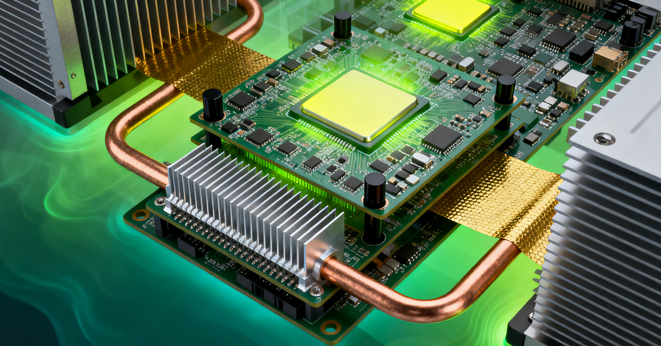
Advanced PCB Thermal Management represents a paradigm shift from isolated cooling fixes to holistic system optimization, addressing the thermal challenges of power-dense, miniaturized electronics. Unlike traditional thermal solutions that focus on single components (e.g., heatsinks or thermal vias), this advanced approach integrates thermal design with electrical performance, mechanical reliability, and manufacturing feasibility—creating a cohesive ecosystem where heat dissipation enhances, rather than compromises, overall product functionality. As electronics push into extreme environments (e.g., space, industrial automation) and edge computing drives demand for compact, high-performance devices, Advanced PCB Thermal Management has become a critical enabler of innovation. This article explores its system-level design principles, emerging technology integrations, cross-industry adaptive strategies, and the future of thermal engineering for PCBs.
At its core, advanced thermal management relies on three interconnected system-level principles:
Designs no longer treat thermal, electrical, and mechanical requirements as separate silos. For example, routing high-current traces alongside thermal planes balances signal integrity and heat dissipation, while optimizing PCB thickness ensures mechanical stability without restricting heat flow. This synergy prevents tradeoffs—such as a thermal via array that doesn’t disrupt sensitive circuitry or a heat spreader that doesn’t add excessive weight.
Instead of reactive cooling, advanced systems use predictive tools to map heat generation during the early design phase. Engineers simulate how components (e.g., CPUs, power ICs) interact thermally, identifying potential hotspots before prototyping. This proactive approach eliminates costly redesigns and ensures thermal solutions are tailored to actual heat profiles, not worst-case guesses.
Heat flow is optimized across micro (component pad), meso (PCB layer), and macro (system-level cooling) scales. For instance, micro-scale thermal vias direct heat from a power transistor’s pad to a meso-scale copper plane, which then feeds into a macro-scale liquid cooling loop. This multi-scale alignment minimizes thermal resistance at every stage, ensuring efficient heat migration from source to sink.

Advanced PCB Thermal Management leverages cutting-edge technologies to push performance boundaries:
Machine learning algorithms analyze vast datasets from past designs and real-world thermal tests to optimize layouts automatically. For example, AI tools can adjust thermal via placement, copper pour patterns, or component positioning to reduce hotspots by 30%—all while preserving electrical performance. These tools also adapt to design changes in real time, re-simulating thermal effects within minutes.
Integrated IoT sensors embedded in PCBs track temperature fluctuations during operation, sending data to a central system. This allows for dynamic cooling adjustments (e.g., activating a low-power fan when a hotspot emerges) or predictive maintenance (alerting to abnormal thermal trends that signal component degradation). For industrial systems, this monitoring ensures uptime by preventing thermal failures before they occur.
Nanocomposite Materials: Graphene or carbon nanotube-reinforced substrates offer 3–5x higher thermal conductivity than traditional FR-4, enabling thinner, lighter PCBs with superior heat dissipation.
3D-Printed Thermal Structures: Additive manufacturing creates complex, customized heat spreaders (e.g., fractal-shaped copper cores) that maximize surface area without increasing PCB footprint. These structures are tailored to specific component heat maps, delivering targeted cooling.

Advanced thermal management adapts to the unique demands of diverse sectors:
Satellite and avionics PCBs face extreme temperature swings (-60°C to 120°C) and vacuum environments. Solutions include phase-change material (PCM) embedded thermal planes that absorb heat during peak operation and release it during cool-down, paired with radiation shields to prevent heat loss in space.
Edge servers and 5G base stations require compact, fan-less thermal solutions. Advanced designs use heat pipes integrated into PCB layers, routing heat to the device chassis (acting as a passive heatsink). Nanocomposite substrates ensure heat is dissipated quickly, even in dense, airflow-restricted enclosures.
Diagnostic equipment (e.g., ultrasound machines) and implantable devices demand low-noise, biocompatible thermal management. Advanced PCB designs use ceramic substrates with integrated copper paths—offering high thermal conductivity without electrical interference—while hermetically sealed thermal enclosures prevent contamination in sterile environments.

The field is evolving to meet the demands of next-gen electronics:
Self-Healing Thermal Paths: Materials that repair micro-cracks in thermal vias or PCBs, maintaining heat flow over long lifespans.
Zero-Emission Cooling: Passive thermal solutions that eliminate the need for energy-consuming fans or pumps, aligning with sustainability goals.
Digital Twin Thermal Modeling: Virtual replicas of PCBs and their operating environments, enabling real-time thermal optimization across the product lifecycle.
Advanced PCB Thermal Management is no longer just about cooling—it’s about designing electronics where thermal efficiency enhances performance, reliability, and scalability. By embracing system-level synergy, AI-driven design, and emerging materials, it solves the thermal challenges of power-dense, extreme-environment electronics. As industries from aerospace to healthcare push the boundaries of what’s possible, advanced thermal management will remain a cornerstone of innovation—proving that effective heat dissipation is as critical as component design for next-gen technology.

Got project ready to assembly? Contact us: info@apollopcb.com


We're not around but we still want to hear from you! Leave us a note:

Leave Message to APOLLOPCB
