-
- PCB TYPE
- PRINTED CIRCUIT BOARD PROTOTYPE ALUMINUM PRINTED CIRCUIT BOARD R&F PCB FPC HIGH FREQUENCY PCB HIGH-TG PCB HEAVY COPPER PCB HDI PCB PCB FOR LIGHTING METAL CORE PCB
time:Jul 14. 2025, 10:12:20
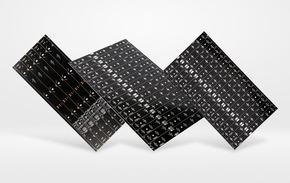
In the realm of high-power, high-density electronics, the 4-layer aluminum PCB stackup has emerged as a sophisticated solution, balancing thermal efficiency, signal integrity, and mechanical robustness. Unlike simpler single or double-layer designs, this multi-layer configuration integrates dedicated layers for power distribution, signal routing, and heat dissipation, making it ideal for applications demanding complex functionality in compact form factors. This article explores the structural composition, material selection, design methodologies, manufacturing processes, and key applications of 4-layer aluminum PCB stackups, highlighting their role in enabling next-generation electronic systems.
Structural Composition of 4-Layer Aluminum PCB Stackup
Layer Configuration and Functional Roles
A 4-layer aluminum PCB stackup features a hierarchical structure optimized for multi-functional performance:
Layer 1 (Top Signal Layer): Primary routing layer for high-speed signals and surface-mount components (e.g., microcontrollers, sensors). This layer directly interfaces with active components, requiring precise trace impedance control for signal integrity.
Layer 2 (Power/Ground Plane): A dedicated copper plane for power distribution or grounding, reducing electromagnetic interference (EMI) and providing a low-impedance return path for signals. When configured as a power plane, it ensures uniform voltage delivery to components across the board.
Layer 3 (Inner Signal/Power Layer): Secondary layer for additional signal routing or auxiliary power paths, enabling separation of analog and digital signals to minimize crosstalk. This layer is particularly useful for complex circuits requiring isolation between sensitive and high-power components.
Layer 4 (Bottom Layer + Aluminum Core): The bottom copper layer, bonded to a thick aluminum substrate via a dielectric layer. This layer supports through-hole components and acts as a thermal anchor, with the aluminum core dissipating heat from both top and inner layers through thermal vias.
This structure leverages vertical integration to maximize board real estate, accommodating dense component layouts without sacrificing thermal or electrical performance.
Key Advantages Over Lower-Layer Configurations
Enhanced Thermal Distribution: The aluminum core, paired with thermal vias connecting all four layers, creates a 3D heat dissipation network. This ensures heat from inner layers (e.g., power semiconductors) is efficiently transferred to the aluminum substrate, preventing hotspots.
Improved Signal Integrity: Dedicated ground planes in Layer 2 reduce EMI by providing a shielded environment for high-frequency signals on Layers 1 and 3. This is critical for applications like 5G transceivers and industrial sensors, where signal clarity is paramount.
Power Density Optimization: Separate power layers enable parallel current paths, reducing voltage drops in high-current circuits (e.g., motor drives). This allows 4-layer stackups to handle higher power densities than 2-layer designs of the same size.
Design Flexibility: Inner layers facilitate complex routing strategies, such as differential pair isolation and split power domains, supporting mixed-signal systems (e.g., analog sensors paired with digital processors).
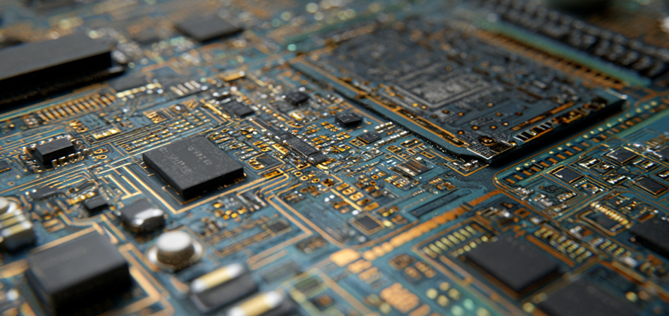
Material Selection for 4-Layer Aluminum PCB Stackups
Aluminum Core: The Thermal Backbone
The aluminum core in 4-layer stackups is selected for:
High Thermal Conductivity: Alloys like 6061 and 6063 balance conductivity with mechanical strength, ensuring efficient heat spread from inner layers to external heat sinks or ambient air.
Thickness Adaptability: Thicker cores enhance heat capacity for high-power applications (e.g., industrial inverters), while thinner variants reduce weight for portable devices (e.g., medical monitors).
Corrosion Resistance: Natural oxide layers or protective coatings (e.g., anodization) shield the core from moisture and chemicals, critical for outdoor or humid environments.
Dielectric Layers: Balancing Insulation and Heat Transfer
Dielectric materials between copper layers and the aluminum core must meet dual requirements:
Electrical Isolation: Materials like ceramic-filled epoxies or polyimides prevent short circuits between conductive layers, with breakdown voltages tailored to the application’s operating voltage.
Thermal Conductivity: High-performance dielectrics (e.g., boron nitride-filled polymers) minimize thermal resistance, ensuring heat from inner copper layers reaches the aluminum core efficiently.
CTE Matching: Dielectrics with coefficients of thermal expansion (CTE) close to aluminum and copper reduce stress during thermal cycling, preventing delamination—a common failure mode in multi-layer PCBs.
Copper Layers: Conductive Pathways with Purpose
Copper layers are optimized based on their role:
Signal Layers (1 and 3): Thin, high-purity copper (e.g., rolled annealed foil) minimizes signal loss in high-frequency circuits, with surface finishes like ENIG (Electroless Nickel Immersion Gold) enhancing solderability and corrosion resistance.
Power/Ground Layers (2 and 4): Thicker copper (relative to signal layers) reduces resistance in current-carrying paths, supporting high-power components like MOSFETs and voltage regulators.
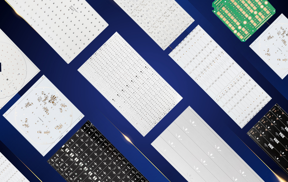
Design Strategies for 4-Layer Aluminum PCB Stackups
Thermal Management: 3D Heat Dissipation
Thermal Via Placement: Through-vias, connecting all four layers, are strategically placed beneath heat-generating components (e.g., power inductors) to create vertical heat channels. Blind vias link surface layers to the aluminum core without penetrating the entire board, preserving inner layer integrity.
Layer-Specific Component Distribution: High-power devices are placed on Layer 4 (adjacent to the aluminum core) for direct heat transfer, while low-power sensors and ICs occupy Layers 1 and 3, reducing thermal interference.
Heat Sink Integration: The exposed aluminum core on Layer 4 can be directly coupled to external heat sinks, with thermal interface materials (TIMs) filling micro-gaps to enhance conduction.
Signal Integrity: Isolation and Routing
Ground Plane Utilization: Layer 2 acts as a solid ground plane, providing a low-impedance return path for signals on Layers 1 and 3. This minimizes loop area, reducing EMI radiation and susceptibility.
Differential Pair Routing: High-speed signals (e.g., USB 3.2, Ethernet) are routed as differential pairs on Layers 1 or 3, with controlled impedance maintained via trace width, spacing, and dielectric thickness.
Analog-Digital Separation: Inner Layer 3 can be dedicated to analog signals, while Layer 1 handles digital circuits, with the ground plane in Layer 2 preventing cross-talk between domains.
Power Distribution: Efficient Current Delivery
Parallel Power Paths: Layer 2 (primary power plane) and Layer 4 (secondary power path) distribute current in parallel, reducing resistance and voltage drop in high-current circuits (e.g., EV motor controllers).
Decoupling Capacitor Placement: Ceramic capacitors are placed on Layers 1 and 4, close to IC power pins, with vias connecting them to the power plane in Layer 2. This stabilizes voltage supply and filters high-frequency noise.
Split Power Domains: Inner Layer 3 can be divided into isolated regions for different voltage levels (e.g., 3.3V and 5V), preventing interference between sensitive analog and high-voltage digital circuits.
Mechanical Design: Stability Under Stress
Layer Thickness Balancing: Symmetric layer stacking (e.g., equal copper thickness on Layers 1 and 4) minimizes warping during thermal cycling, critical for automated assembly and long-term reliability.
Edge Reinforcement: Reinforced edges or stiffeners prevent flexing in large boards, protecting solder joints and via connections in vibration-prone environments (e.g., automotive electronics).
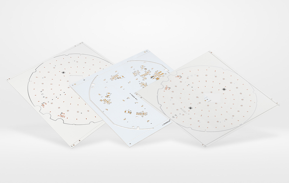
Manufacturing Processes for 4-Layer Aluminum PCB Stackups
Layer Preparation and Lamination
Core Treatment: The aluminum core undergoes surface etching to enhance dielectric adhesion, followed by cleaning to remove oxides and contaminants.
Sequential Lamination: Layers are bonded in stages: first, the dielectric and copper for Layer 4 are laminated to the aluminum core; then, inner layers (2 and 3) are added with dielectric interlayers; finally, Layer 1 is bonded. Each lamination step uses controlled temperature and pressure to eliminate voids.
Adhesive Selection: Low-outgassing adhesives are used for high-reliability applications (e.g., aerospace), preventing dielectric degradation under vacuum or extreme temperatures.
Via Formation and Plating
Drilling: Mechanical or laser drilling creates via holes, with laser drilling preferred for microvias connecting inner layers without damaging the aluminum core.
Desmearing and Plating: Via walls are cleaned (desmeared) to remove dielectric residue, then plated with copper to ensure electrical continuity between layers. Thicker plating in power vias enhances current-carrying capacity.
Circuit Patterning and Etching
Photolithography: Circuit patterns are transferred to each copper layer using photoresists, with laser direct imaging (LDI) ensuring high precision for fine-pitch traces (≤50μm) on signal layers.
Etching: Chemical etching removes unwanted copper, with etch-stop techniques protecting inner layers during processing.
Surface Finishing and Testing
Selective Finishing: Layer 1 (component side) receives ENIG or OSP (Organic Solderability Preservative) for solderability, while Layer 4 (aluminum side) may be left exposed or coated with a conformal layer for corrosion resistance.
Electrical Testing: Flying probe testers verify continuity and isolation between layers, with boundary scan testing for complex ICs. Thermal imaging under load confirms uniform heat distribution across all layers.
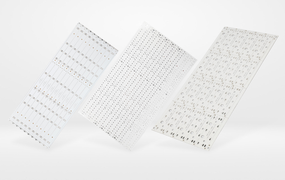
Applications of 4-Layer Aluminum PCB Stackups
Industrial Power Electronics
Motor Drives and Inverters: The 4-layer stackup supports high-current power paths (Layers 2 and 4) and isolated control signals (Layers 1 and 3), enabling compact designs for AC motor controllers and solar inverters.
Uninterruptible Power Supplies (UPS): Dedicated power layers handle battery charging/discharging currents, while signal layers manage monitoring and protection circuits, ensuring reliable backup power.
Automotive Electronics
EV On-Board Chargers (OBCs): The aluminum core dissipates heat from high-voltage rectifiers, with 4-layer isolation separating primary and secondary circuits to meet safety standards (e.g., IEC 61851).
ADAS Control Modules: Dedicated ground planes reduce EMI in radar and camera interfaces, while inner layers isolate sensor signals from power management circuits, enhancing detection accuracy.
High-End LED Systems
Stage Lighting and Projectors: 4-layer stackups accommodate dense LED arrays on Layer 4 (near the aluminum core) and dimming control circuits on Layers 1 and 3, balancing thermal management with complex functionality.
UV-C Sterilization Devices: Isolated power layers handle high-voltage UV drivers, while signal layers manage safety interlocks, ensuring reliable operation in healthcare and food processing applications.
Medical Devices
Portable Ultrasound Machines: The stackup’s compact form factor and thermal efficiency support battery-powered operation, with isolated analog layers preserving signal integrity in transducer interfaces.
Patient Monitors: Separate power and signal layers prevent noise in vital sign sensors, while the aluminum core dissipates heat from processing units, ensuring reliability in 24/7 clinical environments.
Emerging Trends in 4-Layer Aluminum PCB Design
Advanced Dielectric Materials
Nano-Composite Dielectrics: Additives like graphene or carbon nanotubes enhance thermal conductivity of dielectric layers, enabling higher power densities without increasing board size.
Low-Loss Polymers: PTFE-based dielectrics with ultra-low dissipation factors are being integrated for 6G and mmWave applications, supporting signal integrity above 100 GHz.
Miniaturization and HDI Integration
Microvia Technology: Laser-drilled microvias (≤50μm diameter) enable finer pitch routing, supporting component densities up to 2x higher than traditional 4-layer designs—critical for wearable electronics and IoT sensors.
Buried Components: Passive components (resistors, capacitors) are embedded in inner layers, reducing surface area and improving thermal proximity to the aluminum core.
Sustainable Manufacturing
Recycled Aluminum Cores: Post-consumer recycled aluminum, processed to maintain thermal conductivity, reduces lifecycle environmental impact without performance trade-offs.
Eco-Friendly Etching: Acid-free etching processes minimize chemical waste, aligning with automotive and consumer electronics sustainability mandates (e.g., EU REACH).
Simulation-Driven Design
AI-Optimized Stackups: Machine learning algorithms analyze thermal, electrical, and mechanical data to optimize layer thicknesses, via placement, and component distribution, reducing design iterations by up to 30%.
Multiphysics Simulation: Tools integrating thermal, EMI, and structural analysis ensure stackups meet performance targets before prototyping, critical for high-cost applications like aerospace.
Conclusion
The 4-layer aluminum PCB stackup represents a pinnacle of electronic design, combining vertical integration, thermal efficiency, and signal integrity to meet the demands of high-power, high-density devices. By leveraging dedicated layers for power, ground, and signals—all anchored to a thermally conductive aluminum core—these stackups enable innovations in industries ranging from automotive to healthcare. As materials and manufacturing techniques advance, 4-layer aluminum PCBs will continue to evolve, supporting higher frequencies, greater power densities, and more sustainable designs. For engineers, mastering their design principles is essential to unlocking the full potential of next-generation electronic systems, where performance and reliability are non-negotiable.

Got project ready to assembly? Contact us: info@apollopcb.com


We're not around but we still want to hear from you! Leave us a note:

Leave Message to APOLLOPCB
