-
- PCB TYPE
- PRINTED CIRCUIT BOARD PROTOTYPE ALUMINUM PRINTED CIRCUIT BOARD R&F PCB FPC HIGH FREQUENCY PCB HIGH-TG PCB HEAVY COPPER PCB HDI PCB PCB FOR LIGHTING METAL CORE PCB
time:Jun 25. 2025, 09:52:38
In the dynamic realm of electronics, the continuous pursuit of smaller, more powerful, and energy - efficient devices has led to a significant increase in heat generation within electronic components. This heat, if not managed effectively, can cause performance degradation, reduced lifespan, and even system failures. Aluminum Printed Circuit Boards (PCBs) have emerged as a crucial solution in addressing these thermal challenges.
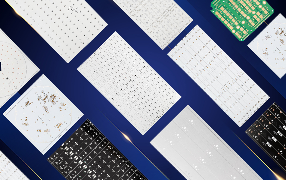
Aluminum PCBs are a type of metal - core PCB that combines the electrical conductivity of traditional PCBs with the excellent thermal conductivity of aluminum. This unique combination allows for efficient heat dissipation from high - power components, such as LEDs, power transistors, and integrated circuits. As a result, aluminum PCBs have found widespread applications in various industries, including lighting, automotive, aerospace, and consumer electronics.
Structure and Components of Aluminum PCBs
Aluminum Substrate
The aluminum substrate forms the foundation of an aluminum PCB. Aluminum is chosen for its high thermal conductivity, which is approximately 200 - 237 W/(m·K) for common alloys like 6061 and 7075. This high thermal conductivity enables the substrate to quickly absorb and transfer heat away from heat - generating components.
The substrate is typically made of an aluminum alloy sheet, which provides mechanical support to the PCB. The thickness of the substrate can vary depending on the application requirements, with common thicknesses ranging from 0.8 mm to 3.2 mm. Thicker substrates offer better thermal performance but may increase the weight and cost of the PCB.
Dielectric Layer
Lying between the aluminum substrate and the copper traces is the dielectric layer. The dielectric layer serves two primary functions: electrical insulation and thermal conduction. It prevents electrical short - circuits between the copper traces and the aluminum substrate while allowing heat to flow from the components through the copper traces and into the aluminum substrate.
Common materials used for the dielectric layer in aluminum PCBs include thermally conductive polymers and composites. These materials are formulated to have high dielectric strength to withstand the electrical voltages present in the circuit. Additionally, they are filled with thermally conductive fillers, such as aluminum oxide or boron nitride, to enhance their thermal conductivity. The thickness of the dielectric layer is carefully controlled to balance electrical insulation and thermal performance, typically ranging from 0.05 mm to 0.2 mm.
Copper Traces
The copper traces on an aluminum PCB are responsible for carrying the electrical current to the components. Copper is an ideal material for this purpose due to its high electrical conductivity, with a conductivity of approximately 58 MS/m. High - purity copper is used to minimize resistance in the traces, which helps to reduce power losses and ensures that the components receive a stable and efficient power supply.
The layout of the copper traces is designed to meet the specific electrical requirements of the components. In a typical aluminum PCB, the traces are routed to connect the power source to the components in a way that evenly distributes the current. The width and thickness of the copper traces are determined based on the amount of current they need to carry. Thicker traces can handle higher currents but may also increase the cost and size of the PCB. Therefore, a balance must be struck between current - carrying capacity and cost - effectiveness.
Manufacturing Process of Aluminum PCBs
Material Preparation
The manufacturing process of aluminum PCBs begins with the careful selection and preparation of materials. High - quality aluminum sheets with the appropriate alloy composition are chosen based on the thermal and mechanical requirements of the PCB. These sheets are then cut to the desired size and shape for the substrate.
The dielectric material, usually in the form of a pre - impregnated film or a liquid resin, is prepared. Pre - impregnated films are made by impregnating a base material, such as fiberglass, with a thermosetting resin and are cured to a semi - cured state for easy handling and lamination. Liquid resins are mixed with fillers and additives to achieve the desired electrical and thermal properties. High - purity copper foils are selected for the traces and undergo surface treatment to improve adhesion to the dielectric layer.
Lamination
Lamination is the process of bonding the aluminum substrate, dielectric layer, and copper foils together to form a single, cohesive structure. This is typically accomplished using heat and pressure in a laminator. The heat activates the thermosetting resin in the dielectric layer, causing it to flow and bond with the aluminum substrate and copper foils. The pressure ensures that the layers are in close contact, eliminating air gaps and voids.
Precise control of the lamination temperature, pressure, and time is crucial to achieve a high - quality bond. Different lamination techniques, such as vacuum lamination or press lamination, may be used depending on the specific requirements of the PCB. After lamination, the PCB is cooled and trimmed to the final dimensions.
Drilling and Plating
Following lamination, holes are drilled for vias, component mounting, and electrical connections. High - precision drilling machines are used to ensure accurate hole placement and clean hole walls. The drilled holes are then electroplated with copper to create electrical connections between the layers of the PCB.
Electroplating involves immersing the PCB in an electrolyte solution containing copper ions and applying an electric current. The copper ions are deposited on the surface of the holes and the copper traces, forming a continuous layer of copper. The thickness of the copper plating is carefully controlled to ensure proper electrical conductivity and mechanical strength.
Circuit Patterning
Circuit patterning is the process of creating the electrical circuits on the copper layers of the PCB. Photolithography is commonly used for this purpose. A photosensitive resist is applied to the copper surface, which is then exposed to ultraviolet (UV) light through a patterned mask. The areas of the resist exposed to UV light undergo a chemical change, making them soluble in a developer solution.
After development, the exposed copper areas are etched away using an etching solution, leaving behind the desired copper traces. This process requires high precision to ensure accurate trace widths, clearances, and the absence of shorts or open circuits. Advanced photolithography techniques and equipment are used to achieve the required level of precision in circuit patterning.
Surface - Mount Assembly
The surface - mount assembly process involves placing the components onto the PCB. Automated pick - and - place machines are used to precisely position the components on the designated pads on the PCB. The components are then soldered to the PCB using reflow soldering or wave soldering techniques.
Reflow soldering is commonly used for surface - mount assembly. In this process, the PCB with the placed components is passed through a reflow oven, where the solder paste melts and bonds the components to the PCB. Proper control of the temperature profile in the reflow oven is essential to ensure good solder joints and reliable electrical connections.
Testing and Quality Control
After assembly, the aluminum PCBs undergo a series of tests to ensure their functionality and quality. Electrical tests, such as continuity testing, voltage and current testing, and insulation resistance testing, are performed to verify the integrity of the electrical circuits. Thermal tests are conducted to measure the heat dissipation performance of the PCB.
Visual inspection is also carried out to check for any physical defects, such as solder bridges, missing components, or damaged traces. Automated optical inspection (AOI) and X - ray inspection can be used for more detailed and accurate quality control. Any defective PCBs are identified and either repaired or discarded to ensure that only high - quality products are delivered to customers.
Advantages of Aluminum PCBs
Superior Heat Dissipation
One of the most significant advantages of aluminum PCBs is their exceptional heat - dissipation capabilities. The high thermal conductivity of the aluminum substrate allows heat to be quickly transferred away from heat - generating components. This is crucial because excessive heat can cause components to degrade in performance over time, leading to a decrease in efficiency and lifespan.
By maintaining the components at a lower operating temperature, aluminum PCBs can extend the lifespan of the components significantly. In some cases, the lifespan of components in an aluminum - PCB - based system can be up to three times longer than in a traditional FR - 4 PCB - based system. This not only reduces the frequency of replacement but also lowers the overall cost of ownership for the end - user.
Compact and Lightweight Design
The combination of a thin aluminum substrate and surface - mount components enables a highly compact and lightweight design for PCBs. The thin and lightweight nature of the aluminum substrate reduces the overall weight of the PCB, making it more suitable for applications where weight is a critical factor, such as in aerospace and portable electronics.
The compact design also allows for a higher density of components to be placed on the PCB, increasing the functionality and performance of the electronic device. This is especially important in applications where space is limited, such as in smartphones, tablets, and wearable devices.
Energy Efficiency
Aluminum PCBs contribute to energy efficiency in electronic devices. By effectively dissipating heat, they allow components to operate at their optimal efficiency. When components are not overheated, they can convert a higher percentage of electrical energy into useful work, reducing power consumption and energy waste.
In addition, the long lifespan of components in aluminum - PCB - based systems means that there is less need for frequent replacements, which also contributes to overall energy savings. This makes aluminum PCBs an environmentally friendly choice for electronic applications.
High Reliability
The robust construction of aluminum PCBs makes them highly reliable. The aluminum substrate provides a stable and rigid base for the components, protecting them from mechanical stress, vibration, and shock. The multi - layer structure of the PCB, with its carefully designed dielectric and copper trace layers, ensures the integrity of the electrical circuits.
Furthermore, the superior heat - dissipation capabilities of the aluminum PCB prevent thermal stress on the components, reducing the likelihood of component failure. This high level of reliability makes aluminum PCBs suitable for applications where continuous and reliable operation is essential, such as in industrial control systems, medical devices, and automotive electronics.
Design Considerations for Aluminum PCBs
Thermal Design
Component Placement
Proper placement of heat - generating components on the aluminum PCB is crucial for effective heat dissipation. Components should be positioned in a way that maximizes their contact with the aluminum substrate. This can be achieved by placing them directly over thermal vias or in areas of the PCB with high thermal conductivity.
Thermal vias are small holes drilled through the PCB that are filled with a conductive material, usually copper. They provide an additional path for heat to flow from the components to the aluminum substrate. By placing components near thermal vias, heat can be quickly transferred away from the components, reducing their operating temperature. In addition, the layout of components should be designed to ensure even heat distribution across the PCB. Avoiding clustering of high - power components in a single area helps to prevent the formation of hotspots, which can lead to uneven performance and reduced component lifespan.
Thermal Via Design
The design of thermal vias is an important aspect of the thermal design of aluminum PCBs. The size, number, and distribution of thermal vias need to be carefully optimized to ensure efficient heat transfer. Larger thermal vias can transfer more heat, but they also take up more space on the PCB, which may affect the layout of other components.
The number of thermal vias should be sufficient to handle the heat generated by the components. The distribution of thermal vias should be based on the heat - generation patterns of the components. In areas where more heat is generated, such as near high - power components, more thermal vias should be placed. Advanced manufacturing techniques, such as blind and buried vias, can be used to improve the thermal performance of the PCB. Blind vias connect the outer layers of the PCB to an internal layer, while buried vias connect two internal layers. These types of vias can provide more efficient heat transfer paths without taking up additional surface space on the PCB.
Heat - Sink Integration
In some high - power applications, integrating a heat sink with the aluminum PCB can further enhance heat dissipation. A heat sink is a component with a large surface area that is designed to transfer heat from the PCB to the surrounding environment. When integrating a heat sink, it is important to ensure good thermal contact between the heat sink and the aluminum substrate.
Thermal interface materials, such as thermal paste or pads, are used to fill the gaps between the heat sink and the aluminum substrate, improving heat transfer efficiency. The design of the heat sink, including its size, shape, and fin configuration, should be tailored to the specific heat - dissipation requirements of the electronic device. A well - designed heat - sink integration can significantly improve the performance and lifespan of the components, while also considering factors such as cost, size, and aesthetics.
Electrical Design
Trace Routing
The routing of copper traces on the aluminum PCB is critical for ensuring reliable electrical performance. The traces should be routed to minimize resistance, inductance, and capacitance, especially in high - current applications. Short and wide traces are preferred to reduce resistance and power losses. Sharp corners and bends in the traces should be avoided as they can increase inductance and cause signal integrity issues.
In addition, proper separation of power and signal traces is essential to prevent electromagnetic interference (EMI). Power traces carry the high - current power supply to the components, while signal traces carry control signals. By separating these traces, the risk of EMI is reduced, ensuring stable operation of the electronic device. Shielding techniques, such as using ground planes or shielding layers, can also be employed for sensitive signal traces to further enhance signal integrity.
Power and Ground Plane Design
A well - designed power and ground plane is crucial for stable power distribution and reduced EMI in aluminum PCBs. The power plane provides a low - impedance path for the power supply to the components, ensuring a stable and consistent voltage. The ground plane serves as a reference for the electrical circuits and helps to reduce EMI by providing a return path for the current.
To minimize voltage drops and improve power distribution, the power and ground planes should be as large as possible. Decoupling capacitors should be strategically placed near the components to filter out high - frequency noise and stabilize the power supply. Proper grounding techniques, such as star grounding or single - point grounding, can also be implemented to reduce EMI and improve the overall electrical performance of the PCB.
Design for Manufacturability
Designing aluminum PCBs with manufacturability in mind is essential for cost - effective production. Using standard component packages and footprints simplifies the procurement process and reduces the risk of errors during assembly. Avoiding complex shapes and geometries in the PCB design makes the manufacturing process more straightforward, reducing production time and costs.
The design should also be compatible with the selected manufacturing processes, such as surface - mount technology (SMT) assembly, soldering, and testing. Clear design guidelines and specifications should be provided to the manufacturing team to ensure consistent and high - quality production. Consideration of factors such as solderability, component placement accuracy, and testability during the design phase can significantly improve the overall manufacturing efficiency.
Applications of Aluminum PCBs
Lighting Industry
Aluminum PCBs have become the standard in the lighting industry, especially for high - power LED lighting applications. LEDs are highly energy - efficient but generate a significant amount of heat during operation. Aluminum PCBs provide the necessary thermal management to ensure that the LEDs operate at optimal temperatures, extending their lifespan and maintaining their performance.
In architectural lighting, aluminum - PCB - based LED modules are used to create stunning visual effects and enhance the aesthetics of buildings. They can be used for general illumination, accent lighting, and decorative lighting. In automotive lighting, aluminum PCBs are used in headlights, taillights, and interior lighting, providing improved energy efficiency, longer lifespan, and better lighting performance.
Automotive Electronics
The automotive industry is increasingly adopting aluminum PCBs in various electronic systems. In engine control units (ECUs), power electronics, and infotainment systems, aluminum PCBs help to manage the heat generated by high - power components. The high reliability and compact design of aluminum PCBs make them suitable for use in the harsh environment of an automotive application, where they may be exposed to vibration, temperature changes, and moisture.
In electric and hybrid vehicles, aluminum PCBs are used in battery management systems (BMS) to monitor and control the charging and discharging of the battery. The efficient heat dissipation provided by aluminum PCBs helps to ensure the safe and reliable operation of the BMS, which is critical for the performance and lifespan of the battery.
Aerospace and Defense
In the aerospace and defense industries, where reliability and performance are of utmost importance, aluminum PCBs are widely used. In avionics systems, radar systems, and communication systems, aluminum PCBs provide the necessary thermal management and electrical performance. The lightweight and compact design of aluminum PCBs also make them suitable for use in aircraft and spacecraft, where weight and space are critical factors.
Aluminum PCBs are also used in military applications, such as missile guidance systems, weapon systems, and surveillance systems. The high reliability and resistance to environmental stress make them ideal for use in military equipment, which often operates in harsh and demanding conditions.
Consumer Electronics
In the world of consumer electronics, aluminum PCBs are used in a variety of products, such as smartphones, tablets, laptops, and televisions. In smartphones, aluminum PCBs are used for the main board and the battery charging circuit, providing efficient heat dissipation and reliable electrical performance. The compact and lightweight design of aluminum PCBs allows for a thinner and lighter form factor, which is highly desirable in consumer electronics.
In laptops and tablets, aluminum PCBs are used in the power management circuit and the graphics processing unit (GPU), helping to manage the heat generated by these high - power components. In televisions, aluminum PCBs are used in the backlight unit, providing efficient heat dissipation for the LEDs and improving the overall picture quality.

Got project ready to assembly? Contact us: info@apollopcb.com


We're not around but we still want to hear from you! Leave us a note:

Leave Message to APOLLOPCB
