-
- PCB TYPE
- PRINTED CIRCUIT BOARD PROTOTYPE ALUMINUM PRINTED CIRCUIT BOARD R&F PCB FPC HIGH FREQUENCY PCB HIGH-TG PCB HEAVY COPPER PCB HDI PCB PCB FOR LIGHTING METAL CORE PCB
time:Sep 17. 2025, 09:55:51
In the world of electronics, speed is everything. Whether it's your computer, smartphone, or any other device, faster is always better. One of the key components that determine the speed of these devices is the printed circuit board, or PCB. When it comes to high-speed applications, one technique that stands out is backdrilling. But what exactly is backdrilling in PCB manufacturing, and why is it important for high-speed applications? Let's dive into the details.
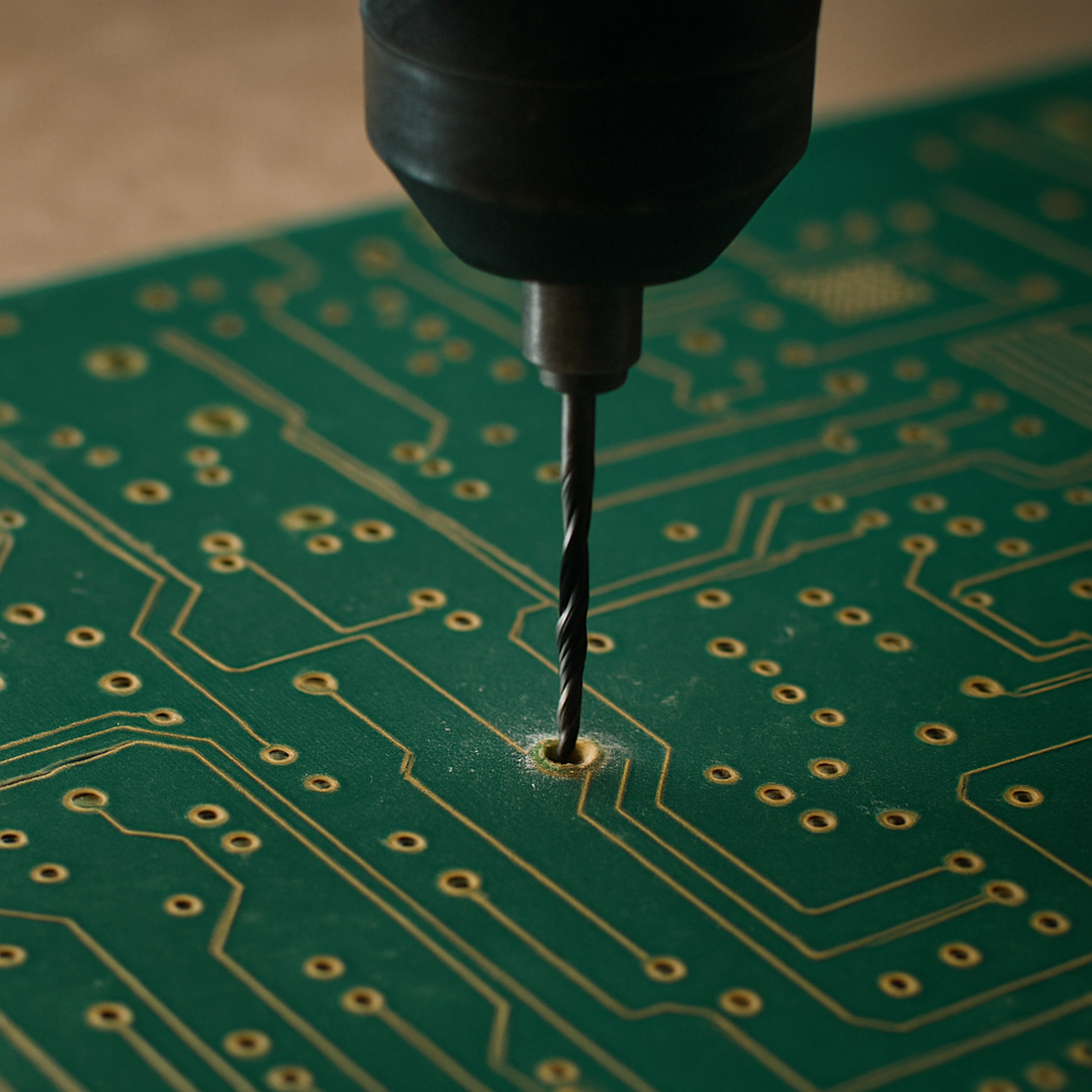
Backdrilling is a specialized technique used during PCB manufacturing to remove unused sections of plated through holes (PTHs). These sections, often called "stubs," can cause signal integrity issues, especially in high-speed applications. By removing these stubs, you improve the performance of the PCB by reducing signal reflections and loss.
In high-speed PCBs, signals travel at incredibly fast rates. Any interruption or impedance can cause significant signal degradation. Stubs in PTHs act like unwanted antennas, reflecting signals back into the system. This can lead to data errors and loss of signal integrity. Backdrilling effectively eliminates these stubs, ensuring cleaner and more accurate signal transmission.

Identifying the Stubs: The first step in backdrilling is to identify which PTHs have stubs that need removal. This is typically done using design software that maps out the entire PCB layout.
Setting the Drill Parameters: Once the stubs are identified, parameters for the backdrilling process are set. This includes the depth and diameter of the drill to ensure only the unwanted stub is removed.
Performing the Backdrill: Using precision drilling equipment, the backdrilling process is performed. The drill carefully removes the stub without affecting the rest of the via or the surrounding areas.
Inspection and Testing: After backdrilling, the PCB is inspected to ensure that the stubs are completely removed. Electrical testing may also be conducted to confirm improved signal integrity.
Improved Signal Integrity: By eliminating stubs, backdrilling significantly enhances signal clarity, reducing the risk of signal degradation.
Better Performance: High-speed applications benefit from backdrilling as it supports faster and more reliable data transmission.
Reduced EMI: Backdrilling helps in reducing electromagnetic interference (EMI), which is crucial for maintaining signal quality.

Backdrilling is especially beneficial in applications where signal integrity is paramount. Some common applications include:
In telecommunications, data is transmitted at high speeds over vast distances. Backdrilling ensures that these signals remain strong and clear, reducing the chances of data loss.
For data centers, where large volumes of data are processed and transferred, backdrilling helps maintain the integrity and speed of these signals, ensuring efficient operation.
In aerospace and defense applications, reliability is critical. Backdrilling ensures that the electronic systems in these fields operate with precision and dependability.

When designing a PCB that will undergo backdrilling, it's essential to account for the additional drilling operations. Designers must ensure that there is enough material around the PTH to accommodate the backdrill.
Backdrilling can add to the manufacturing cost of a PCB due to the specialized equipment and additional steps involved. However, the benefits often outweigh these costs, especially in high-speed applications where signal integrity is crucial.
The precision required in backdrilling can be challenging. It requires careful planning and execution to ensure that only the stub is removed without damaging the surrounding areas.
In the realm of high-speed PCBs, backdrilling is an invaluable technique. By removing unnecessary stubs, it enhances signal integrity, reduces EMI, and supports faster, more reliable data transmission. As technology continues to advance, the need for efficient and effective PCB manufacturing techniques like backdrilling will only grow. Whether it's for telecommunications, data centers, or aerospace applications, backdrilling is an essential part of achieving the high-speed performance that modern electronics demand.
By understanding and implementing backdrilling in PCB manufacturing, you can ensure that your electronic devices not only meet but exceed the speed and performance expectations of today's fast-paced world.

Got project ready to assembly? Contact us: info@apollopcb.com


We're not around but we still want to hear from you! Leave us a note:

Leave Message to APOLLOPCB
