-
- PCB TYPE
- PRINTED CIRCUIT BOARD PROTOTYPE ALUMINUM PRINTED CIRCUIT BOARD R&F PCB FPC HIGH FREQUENCY PCB HIGH-TG PCB HEAVY COPPER PCB HDI PCB PCB FOR LIGHTING METAL CORE PCB
time:Sep 17. 2025, 09:59:18
Printed circuit boards (PCBs) are the backbone of modern electronics, enabling the functionality of devices ranging from smartphones to complex computing systems. Among the various techniques used in PCB manufacturing, controlled depth backdrilling is a critical process that enhances signal integrity and reduces electromagnetic interference. In this article, we will delve into the specifics of controlled depth backdrilled PCBs, their advantages, and the manufacturing process involved.
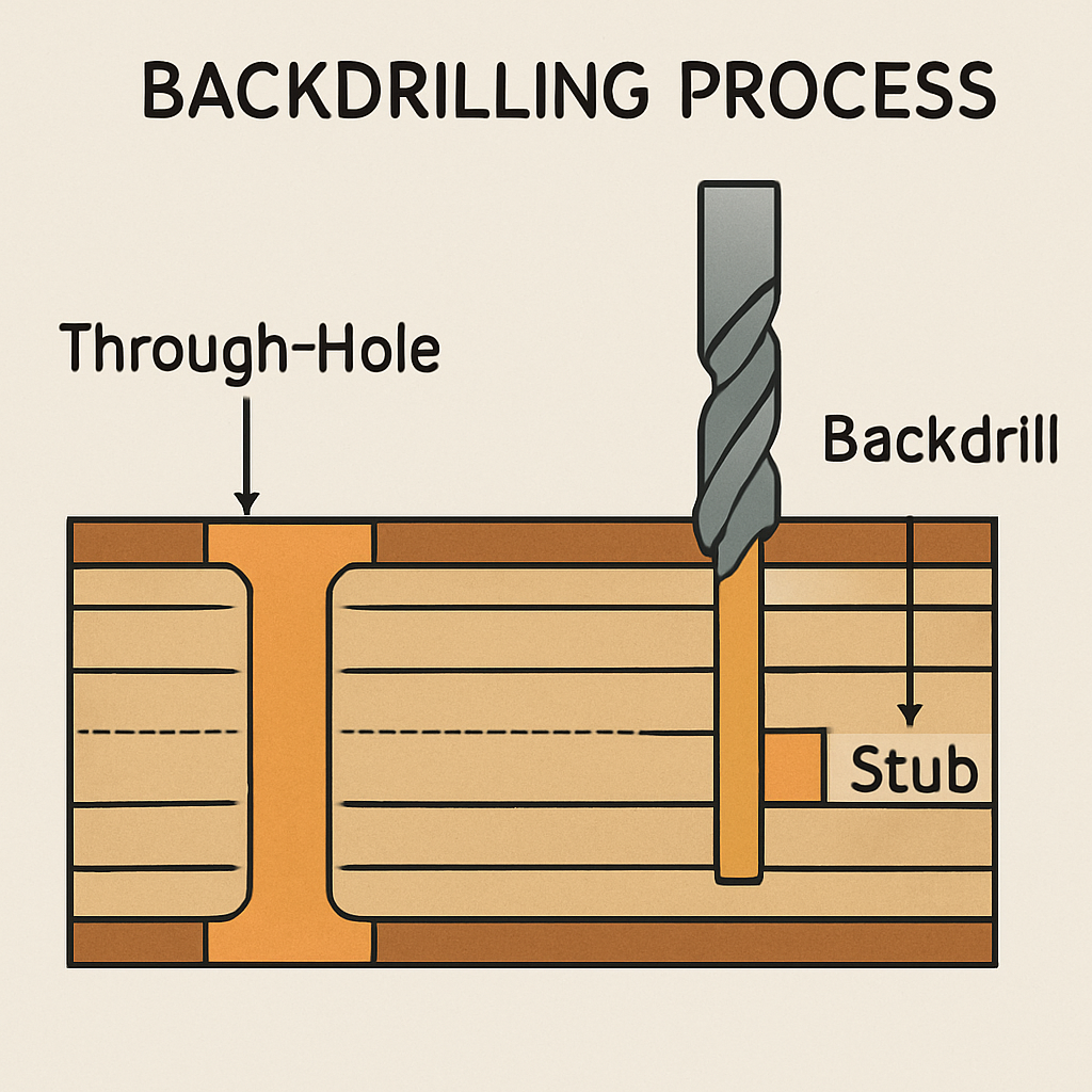
Controlled depth backdrilling is a precision technique used in PCB manufacturing to remove the unused portions of copper-plated through-holes. These through-holes, also known as vias, are used to connect different layers of a PCB. However, in high-speed applications, the unused copper in these vias can cause signal distortion and degrade performance.
Backdrilling involves drilling into the vias to remove the unnecessary sections, which minimizes reflections, reduces stub effects, and improves signal integrity. The term "controlled depth" refers to the precision required to drill to a specific depth without damaging the functional layers of the PCB.

In high-frequency applications, signal integrity is paramount. Unused portions of vias, known as stubs, can act as antennas, leading to signal reflection and loss. By removing these stubs through backdrilling, you can significantly enhance the signal quality and reliability of the PCB.
Electromagnetic interference (EMI) is a common issue in densely packed PCBs. Stubs can contribute to EMI by radiating unwanted signals. Backdrilling helps mitigate this problem by eliminating the stubs, thus reducing potential sources of interference and ensuring that the PCB operates efficiently.
As electronic devices become more advanced, the demand for high-speed data transmission continues to grow. Controlled depth backdrilled PCBs are crucial in these high-speed applications, as they ensure that signal transmission occurs with minimal distortion, thereby maintaining the overall performance of the device.

Before the backdrilling process begins, careful planning and design are essential. Engineers must determine which vias require backdrilling and to what depth. This involves analyzing the PCB layout and understanding the signal paths to avoid drilling into critical areas.
Drilling: The initial step involves drilling the vias as per the PCB design. This creates the necessary connections between the layers.
Plating: Once the vias are drilled, they are plated with copper to ensure electrical conductivity.
Backdrilling: The backdrilling process follows, where a precision drill removes the unwanted copper from the vias. This step requires advanced machinery to achieve the desired depth without affecting the integrity of the surrounding layers.
Inspection: After backdrilling, the PCB undergoes a thorough inspection to ensure that the process has been completed successfully and that no damage has occurred to the functional parts of the board.
The backdrilling process demands high-precision equipment capable of drilling with accuracy to a fraction of a millimeter. Advanced CNC machines are typically used, equipped with specialized drill bits designed for controlled depth operations.

Controlled depth backdrilled PCBs offer superior signal quality due to the elimination of stubs, which can otherwise cause signal degradation. This results in clearer, more reliable data transmission.
By removing unnecessary copper, backdrilling also contributes to better thermal management. This is particularly important in high-density PCBs where heat dissipation is crucial for maintaining performance and longevity.
With the ability to precisely control the depth of drilling, engineers have greater flexibility in designing PCBs. They can optimize the layout for performance without being constrained by the limitations imposed by stubs.
While backdrilling adds an additional step to the manufacturing process, the benefits in terms of improved performance and reduced error rates can lead to cost savings in the long run. Fewer issues mean less rework and higher yields in production.
The need for precision in backdrilling cannot be overstated. Any deviation in depth can lead to damage to the PCB, resulting in costly repairs or replacements. Therefore, skilled technicians and high-quality equipment are essential.
Though beneficial, backdrilling does add to the manufacturing cost. It's important to weigh the advantages of improved performance against the additional expenses involved in the process.
Not all PCBs require backdrilling. It's crucial to assess the specific needs of the application to determine whether controlled depth backdrilling is necessary. This involves considering factors such as operating frequency, signal integrity requirements, and overall design complexity.
Controlled depth backdrilling is a vital process in the world of PCB manufacturing, offering significant enhancements in signal integrity and performance, especially in high-speed applications. While it introduces additional considerations in terms of cost and precision, the benefits in terms of improved reliability and efficiency make it an attractive option for advanced electronics.
As technology continues to evolve and the demand for faster, more reliable electronics grows, controlled depth backdrilled PCBs will remain an essential component in achieving the high standards required in modern electronic devices.

Got project ready to assembly? Contact us: info@apollopcb.com


We're not around but we still want to hear from you! Leave us a note:

Leave Message to APOLLOPCB
