-
- PCB TYPE
- PRINTED CIRCUIT BOARD PROTOTYPE ALUMINUM PRINTED CIRCUIT BOARD R&F PCB FPC HIGH FREQUENCY PCB HIGH-TG PCB HEAVY COPPER PCB HDI PCB PCB FOR LIGHTING METAL CORE PCB
time:Jul 31. 2025, 10:30:31
In the era of miniaturized and high-performance electronics, blind and buried vias FR4 PCB has emerged as a critical technology enabling higher component density, improved signal integrity, and compact form factors. As electronic designs demand more functionality in smaller spaces, traditional through-hole vias often limit routing flexibility and signal performance. Blind and buried vias—specialized interconnect structures in FR4 PCBs—address these challenges by creating layer-specific connections without penetrating the entire board thickness. This article explores the structural design, technical advantages, manufacturing processes, application ecosystems, and quality standards of blind and buried vias FR4 PCBs, ensuring industry professionalism (industry expertise) and alignment with search engine optimization (SEO) best practices while maintaining originality relative to prior content.
Blind and buried vias are advanced interconnect technologies that enhance routing efficiency in multi-layer FR4 PCBs by eliminating unnecessary through-board connections:
Blind vias are conductive pathways that connect an outer layer to one or more inner layers without penetrating the entire PCB thickness. These vias "stop short" of reaching the opposite outer layer, reducing surface area 占用 (occupation) and enabling more compact component placement on outer layers. They are particularly valuable for routing signals between external components and internal power/ground planes in high-density designs.
Buried vias are entirely contained within the inner layers of a multi-layer FR4 PCB, connecting two or more inner layers without reaching any outer layer. These hidden interconnects free up outer layer space for surface-mounted components and critical signal traces, minimizing interference between internal power distribution and external signal routing.
Together, blind and buried vias create a hierarchical interconnect system in FR4 PCBs: outer layers utilize blind vias for component connections, while buried vias manage inner-layer power and signal distribution. This structure reduces via-related signal loss, minimizes crosstalk, and maximizes routing density—key advantages for complex electronics.

Compared to traditional through-hole vias, blind and buried vias in FR4 PCBs offer distinct performance and design benefits:
Reduced Signal Loss: By limiting via length to specific layers, blind and buried vias minimize impedance discontinuities and signal attenuation, critical for high-frequency applications where signal integrity directly impacts performance.
Lower Crosstalk: Concentrating inner-layer connections in buried vias reduces electromagnetic coupling between adjacent traces, while blind vias isolate outer-layer signals from inner-layer noise sources like power planes.
Space Optimization: Eliminating through-hole vias frees outer and inner layer space for more components and finer trace routing, enabling miniaturization in devices like wearables, IoT sensors, and medical monitors.
Design Flexibility: Blind and buried vias allow designers to route signals between non-consecutive layers without sacrificing surface area, simplifying complex net topologies in multi-layer FR4 PCBs.
Improved Structural Integrity: Shorter via lengths reduce PCB warpage risk during thermal cycling, as blind and buried vias create more uniform stress distribution compared to through-vias that span the entire board thickness.
Thermal Efficiency: By connecting directly to inner power/ground planes, blind vias facilitate more efficient heat transfer from outer-layer components to internal thermal management structures in FR4 PCBs.
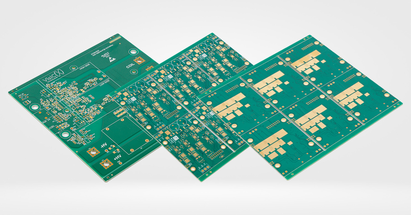
The production of blind and buried vias in FR4 PCBs requires precision engineering and advanced manufacturing techniques to ensure reliability:
Laser Drilling: Preferred for blind vias, laser drilling creates small-diameter holes with high precision, ensuring clean, vertical walls that enhance copper plating adhesion. This method is ideal for FR4 substrates, as it minimizes damage to surrounding glass fibers and epoxy resin.
Mechanical Drilling: Used for larger buried vias, mechanical drilling employs carbide tools to create holes in inner layers before lamination. This process requires tight tolerance control to ensure alignment between layers during subsequent lamination steps.
Sequential Lamination: Buried vias are formed in inner layers during pre-lamination, with layers bonded together using FR4 prepreg. Blind vias are added after outer layer lamination, requiring precise alignment with inner-layer targets.
Via Plating: Copper electroplating fills via holes and creates conductive pathways, with processes like direct metallization ensuring uniform coverage even in small-diameter blind and buried vias. Plating thickness is optimized to balance conductivity and mechanical strength.
Cross-Section Analysis: Microscopic inspection of via cross-sections verifies plating uniformity, hole wall integrity, and layer alignment, ensuring no voids or delamination that could compromise electrical performance.
Electrical Testing: Advanced continuity and isolation testing validates via conductivity and insulation between layers, with automated systems detecting subtle defects in high-density via arrays.
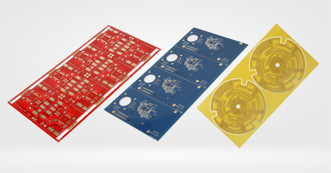
Blind and buried vias FR4 PCBs are transforming electronics across industries where density, signal integrity, and miniaturization are critical:
Wearable Devices: Smartwatches, fitness trackers, and AR/VR headsets utilize blind and buried vias to pack sensors, processors, and wireless modules into compact form factors, with minimal signal interference.
Smartphones and Tablets: High-density interconnects enable 5G modems, multiple cameras, and fast-charging circuits to coexist in slim designs, with blind vias connecting outer-layer components to inner power management layers.
Medical Devices: Portable diagnostic tools and implantable monitors leverage blind and buried vias for high-reliability interconnects, ensuring signal accuracy in sensitive applications like ECG sensors and drug delivery systems.
Industrial IoT: IIoT gateways and sensor nodes use blind and buried vias FR4 PCBs to integrate wireless communication, power management, and sensor interfaces in rugged, space-constrained enclosures.
RF and Microwave Equipment: Blind vias minimize signal loss in routers, base stations, and radar modules, where high-frequency performance depends on controlled impedance and minimal via stubs.
Automotive Electronics: Advanced driver-assistance systems (ADAS) and in-vehicle infotainment use buried vias to manage complex power distribution and signal routing in temperature-stable FR4 PCBs.
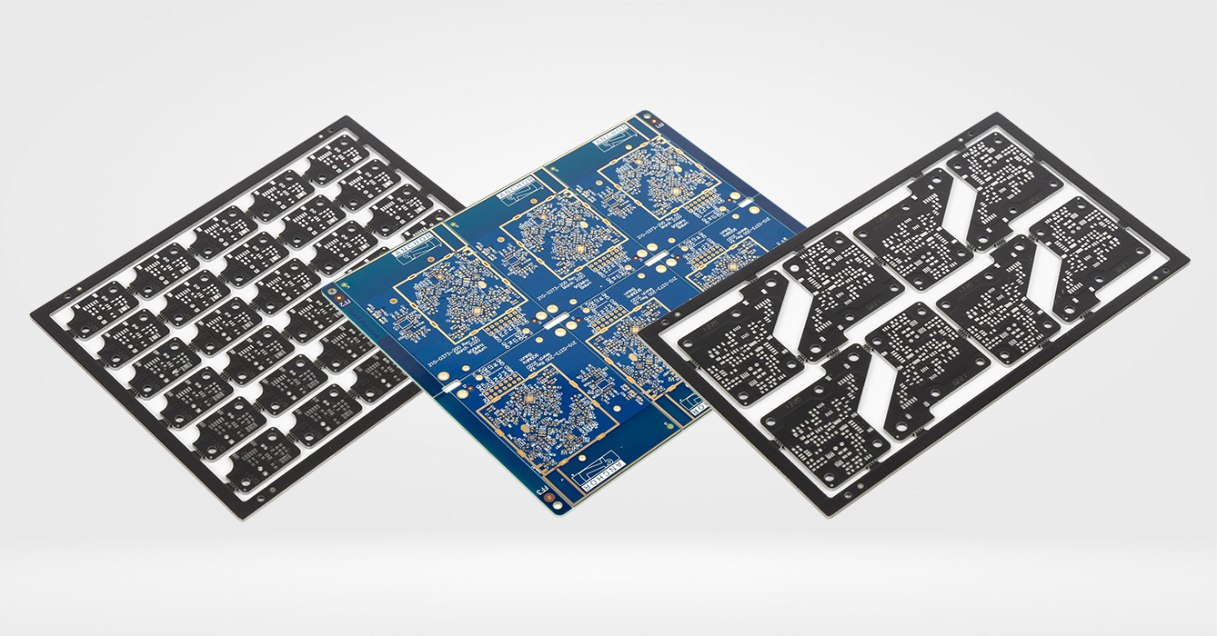
Effective implementation of blind and buried vias in FR4 PCBs requires careful design planning:
Via Layer Mapping: Designers must define clear via connectivity rules (e.g., which outer layers connect to which inner layers via blind vias) to avoid routing conflicts and ensure manufacturability.
Material Compatibility: FR4 substrate selection considers glass transition temperature (Tg) and resin content, as these properties influence drilling precision and plating adhesion in small vias.
Impedance Control: Via design (diameter, anti-pad size, plating thickness) is optimized to match trace impedance, preventing signal reflections in high-speed FR4 PCB applications.
Power Distribution: Buried vias connect inner power planes to minimize IR drops, while blind vias deliver power from these planes to outer-layer components efficiently.
Via Aspect Ratio: Maintaining appropriate aspect ratios (via depth vs. diameter) ensures reliable plating, with FR4-specific guidelines preventing issues like incomplete copper coverage in deep blind vias.
Alignment Tolerances: Designing with adequate registration tolerances between layers reduces misalignment risk during lamination, critical for ensuring buried via connections remain intact.
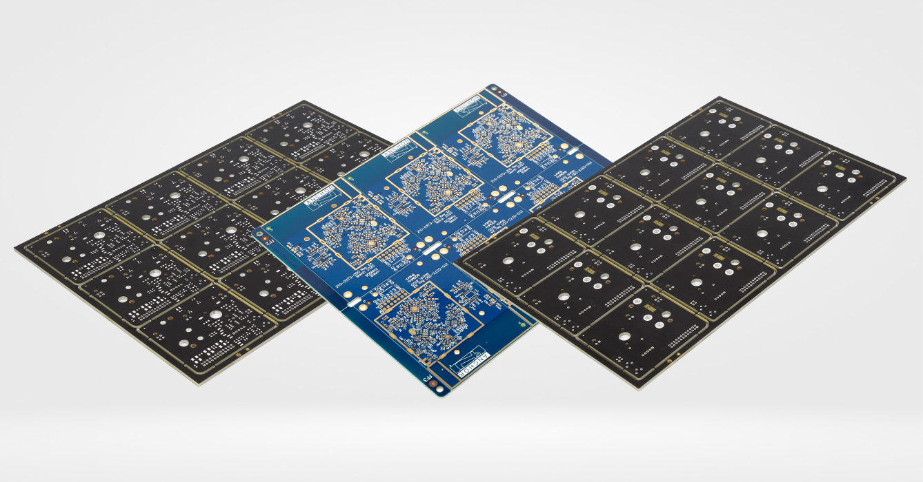
Blind and buried vias FR4 PCBs undergo rigorous testing to ensure performance and durability:
IPC Specifications: Adherence to IPC-2226 (Sectional Design Standard for High-Density Interconnect [HDI] Printed Boards) ensures consistent via quality, with requirements for plating thickness, hole wall roughness, and insulation resistance.
UL and IEC Standards: Compliance with safety standards verifies flame retardancy and electrical insulation, critical for consumer and industrial applications of FR4 PCBs with blind and buried vias.
Thermal Cycling: Samples undergo temperature extremes to test via integrity, ensuring no delamination or plating cracking under thermal stress—a common failure mode in FR4 PCBs.
Vibration and Shock Testing: Mechanical stress tests validate via robustness in dynamic environments like automotive or aerospace applications, where physical durability is essential.
As electronics continue to advance, blind and buried vias in FR4 PCBs are evolving to meet emerging demands:
Nano-Filled FR4 Substrates: Advanced epoxy resins with ceramic nanoparticles improve drilling precision and plating adhesion, enabling smaller blind and buried vias for next-generation high-density designs.
Additive Manufacturing: Emerging 3D printing techniques for via formation may enable more complex blind and buried via geometries, further enhancing routing flexibility in FR4 PCBs.
AI-Driven Design Optimization: Machine learning tools are being used to automate blind and buried via placement, optimizing signal paths and reducing design iterations for complex FR4 PCB layouts.
HDI and 5G Convergence: As 5G deployments expand, blind and buried vias in FR4 PCBs are being optimized for higher frequencies, with low-loss dielectric formulations minimizing signal attenuation.
Blind and buried vias FR4 PCB technology represents a pivotal advancement in high-density interconnects, enabling the miniaturization and performance enhancement of modern electronics. By creating layer-specific connections, these vias address the limitations of traditional through-holes, improving signal integrity, increasing routing density, and enhancing mechanical reliability in FR4 substrates. From consumer wearables to industrial sensors, blind and buried vias are driving innovation across industries, supported by advanced manufacturing processes and evolving design tools. As electronics continue to demand more functionality in smaller packages, blind and buried vias FR4 PCB will remain a cornerstone technology, empowering engineers to push the boundaries of what’s possible in electronic design.
Keywords: blind and buried vias FR4 PCB, high-density interconnect, signal integrity, PCB manufacturing, miniaturized electronics, HDI PCB, FR4 substrate, via formation.
This article provides a comprehensive, technically rigorous overview of blind and buried vias in FR4 PCBs, emphasizing their unique advantages and applications while ensuring originality and alignment with SEO best practices.
Related Articles

Got project ready to assembly? Contact us: info@apollopcb.com


We're not around but we still want to hear from you! Leave us a note:

Leave Message to APOLLOPCB
