-
- PCB TYPE
- PRINTED CIRCUIT BOARD PROTOTYPE ALUMINUM PRINTED CIRCUIT BOARD R&F PCB FPC HIGH FREQUENCY PCB HIGH-TG PCB HEAVY COPPER PCB HDI PCB PCB FOR LIGHTING METAL CORE PCB
time:Dec 17. 2025, 10:24:31
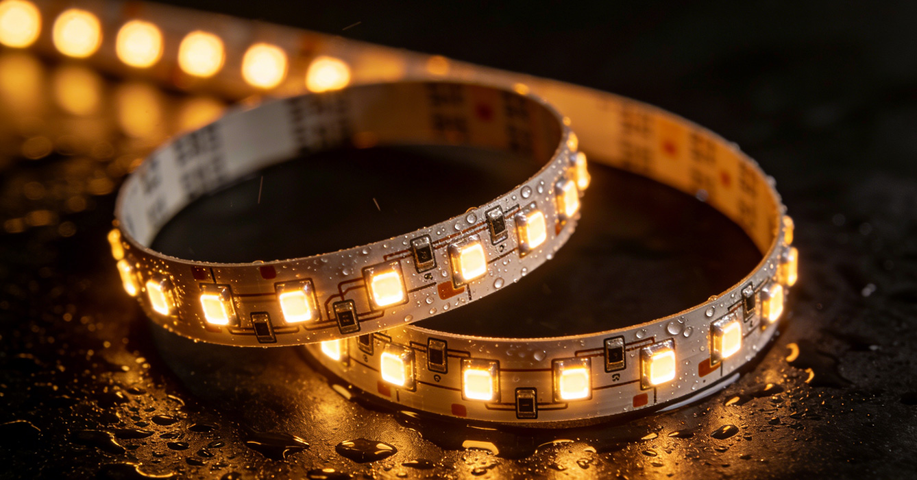
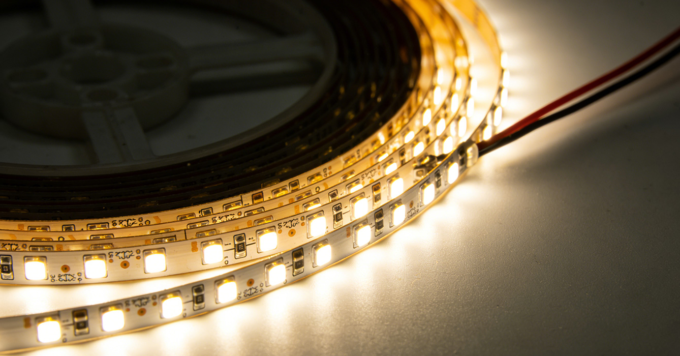
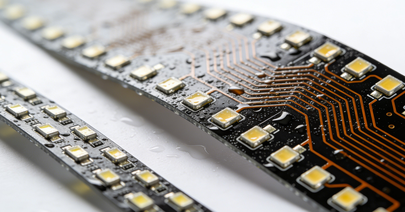
As LED lighting expands into outdoor, marine, automotive, and high-humidity applications, the demand for Waterproof LED Flexible PCB has surged. This specialized circuit solution integrates robust waterproofing technologies with the inherent flexibility and compactness of flexible PCBs, ensuring stable performance of LED systems in moisture, dust, and corrosive environments. Unlike standard flexible PCBs that lack environmental resistance, Waterproof LED Flexible PCB leverages advanced coating, encapsulation, and material optimization to protect LED components and circuit traces from water intrusion and degradation. For lighting manufacturers, adopting high-quality Waterproof LED Flexible PCB is critical to enhancing product durability, reducing maintenance costs, and unlocking new application possibilities in extreme illumination scenarios.
The reliability of Waterproof LED Flexible PCB hinges on sophisticated waterproofing technologies tailored to the unique requirements of LED lighting systems, balancing protection with optical performance and flexibility:
- Nano-Conformal Coatings: Cutting-edge nano-coatings, such as fluorine-based or ceramic-based formulations, provide a ultra-thin, transparent protective layer for LED flexible PCBs. These coatings penetrate tiny gaps and crevices—including between LED chips and circuit traces—forming a 360° waterproof barrier that repels water, oils, and chemicals. The ultra-thin nature of the coating ensures minimal impact on light transmission and maintains the PCB’s flexibility, making it ideal for high-precision LED applications like architectural lighting and display backlights. Additionally, these coatings offer excellent UV resistance, preventing degradation under prolonged outdoor sunlight exposure.
- Encapsulation & Sealing Solutions: For harsh environments with direct water contact, potting and encapsulation technologies are employed. Silicone-based encapsulants are widely used due to their flexibility, thermal stability, and excellent adhesion to PCB substrates. The encapsulation process fully embeds LED components and circuit traces, providing robust protection against water immersion, salt spray, and mechanical impact. Specialized sealing techniques are also applied to connection points and lead-out areas, preventing water ingress at these vulnerable spots. This level of protection is essential for marine lighting, underwater exploration equipment, and industrial washdown areas.
- Corrosion-Resistant Material & Surface Treatment: The substrate and conductive layers of Waterproof LED Flexible PCB are optimized for corrosion resistance. Medical-grade polyimide substrates with UV stabilizers are adopted to withstand extreme temperature fluctuations and environmental aging. For circuit traces and solder pads, surface treatments such as electroless nickel immersion gold (ENIG) or organic solderability preservatives (OSP) replace traditional tin plating, enhancing resistance to oxidation and salt corrosion. These material upgrades extend the service life of LED lighting systems in harsh marine or coastal environments.

Waterproofing measures can hinder heat dissipation, a key challenge for high-power LED systems. Waterproof LED Flexible PCB addresses this through integrated thermal management solutions:
- Thermally Enhanced Substrates: Advanced substrates, such as ceramic-filled polymers or metal-clad flexible materials, are used to improve thermal conductivity while maintaining waterproof performance. These substrates efficiently transfer heat generated by LEDs away from the chip, preventing overheating-induced light decay and component failure. The combination of thermal enhancement and waterproofing ensures stable LED performance even in high-power lighting applications like outdoor floodlights.
- Optimized Trace & Pad Design: The layout of circuit traces and LED pads is engineered to facilitate heat distribution. Wider traces and enlarged thermal pads increase heat dissipation area, while strategic placement of vias creates thermal pathways to dissipate heat from the LED junction to the substrate. This design synergy ensures that waterproofing layers do not trap heat, maintaining the long-term reliability and luminous efficiency of the LED system.

Waterproof LED Flexible PCB enables innovative LED lighting solutions across diverse harsh-environment sectors:
- Outdoor & Landscape Lighting: In architectural accent lighting, garden lighting, and outdoor signage, Waterproof LED Flexible PCB’s flexibility allows it to conform to curved surfaces and irregular shapes, creating dynamic lighting effects. Its waterproof and UV-resistant properties ensure long-term performance in rain, snow, and intense sunlight, reducing the need for frequent maintenance.
- Automotive Lighting Systems: For automotive interior ambient lighting, exterior daytime running lights, and undercarriage lighting, Waterproof LED Flexible PCB withstands vibration, temperature extremes, and exposure to automotive fluids. Its compact size and flexibility enable seamless integration into tight spaces and curved surfaces of vehicle designs, enhancing both aesthetics and functionality.
- Marine & High-Humidity Environments: Marine lighting, bathroom lighting, and industrial wet areas benefit from the corrosion-resistant and waterproof properties of these PCBs. They resist saltwater corrosion, steam, and chemical cleaners, ensuring reliable illumination in environments that would quickly degrade standard LED circuits.

The development of Waterproof LED Flexible PCB is evolving toward sustainable manufacturing and smart functionality integration:
- Sustainable Waterproof Materials: Research is focused on developing eco-friendly waterproof coatings and substrates, such as recyclable silicone and bio-based polymers. These materials maintain high waterproof performance while reducing environmental impact, aligning with global carbon neutrality goals in the lighting industry.
- Smart Sensing Integration: Future designs will integrate environmental sensors (e.g., humidity, temperature) directly into Waterproof LED Flexible PCB, enabling real-time monitoring of operating conditions. This smart functionality allows for adaptive lighting control and predictive maintenance, enhancing the intelligence and efficiency of LED systems.
- Cost-Effective Manufacturing Scalability: Advancements in automated coating and encapsulation processes are reducing production costs of Waterproof LED Flexible PCB, making this technology more accessible for mainstream lighting applications. This scalability will drive wider adoption in residential and commercial lighting markets.
In conclusion, Waterproof LED Flexible PCB is a key enabler of reliable LED lighting in harsh environments, combining advanced waterproofing technologies with thermal management optimization. Its unique capabilities support innovation across outdoor, automotive, and marine lighting sectors, while emerging trends in sustainability and smart integration promise to expand its impact further. As the demand for durable, high-performance LED lighting continues to grow, Waterproof LED Flexible PCB will play an increasingly vital role in shaping the future of the global lighting industry.
[Contact ApolloPCB Today for a Free Review and Precision Quote]

Got project ready to assembly? Contact us: info@apollopcb.com


We're not around but we still want to hear from you! Leave us a note:

Leave Message to APOLLOPCB
