-
- PCB TYPE
- PRINTED CIRCUIT BOARD PROTOTYPE ALUMINUM PRINTED CIRCUIT BOARD R&F PCB FPC HIGH FREQUENCY PCB HIGH-TG PCB HEAVY COPPER PCB HDI PCB PCB FOR LIGHTING METAL CORE PCB
time:Sep 16. 2025, 09:17:12
Printed Circuit Boards (PCBs) are the backbone of modern electronic devices, offering a platform for electrical connections and mechanical support. Among the intricate features of PCBs, vias play a crucial role. In this article, we explore the concept of blind and buried vias, their significance in PCB manufacturing, and their impact on electronic design.
To comprehend blind and buried vias, it's essential to first understand what vias are in the context of PCBs. Vias are small holes drilled through the PCB layers to enable electrical connections between different layers. These are typically filled with conductive material, like copper, to ensure proper electrical conductivity.
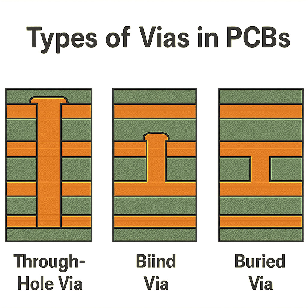
There are three main types of vias used in PCB design:
Through-hole Vias: These extend through the entire PCB, connecting all the layers.
Blind Vias: These connect an outer layer to one or more inner layers but do not go through the entire board.
Buried Vias: These are located entirely within the inner layers of the PCB and do not reach the outer layers.
Blind and buried vias are particularly important in high-density PCB designs. They enable more compact and complex designs by allowing additional routing space and reducing the number of through-hole vias, which can clutter the board.
Space Optimization: By using blind and buried vias, designers can save valuable PCB space, making it possible to create smaller devices.
Improved Signal Integrity: These vias help reduce the electrical path length, which can enhance the signal integrity by minimizing inductance and resistance.
Layer Count Reduction: They allow for the reduction of the overall number of layers required, potentially reducing the cost and weight of the PCB.

The manufacturing process of blind and buried vias is more complex than that of through-hole vias. Here's a brief overview of how they are typically created:
Drilling: The vias are drilled using advanced laser or mechanical drilling techniques. For blind vias, the drill reaches only partway through the board, while for buried vias, it stays within the inner layers.
Plating: After drilling, the vias are plated with copper to establish an electrical connection between the layers.
Precision: The drilling and plating process requires high precision to ensure reliable connections without damaging the board.
Cost: The additional complexity in manufacturing can increase the cost, which is an important consideration in high-volume production.

Blind and buried vias are predominantly used in applications where space and performance are critical. Here are some common applications:
In devices like smartphones and tablets, where space is at a premium, blind and buried vias help reduce the board size while maintaining functionality.
These sectors often require high-performance PCBs with stringent size and weight constraints, making blind and buried vias an ideal solution.
For compact medical devices, such as wearable sensors and portable diagnostic tools, these vias facilitate the necessary miniaturization.

Despite their advantages, using blind and buried vias comes with challenges that need careful consideration:
Integrating blind and buried vias adds complexity to PCB design. Designers must have a thorough understanding of the technology and its implications on the overall layout and performance.
As mentioned, the manufacturing of blind and buried vias is more costly. It's crucial to weigh the benefits against the additional expenses to ensure it's a viable solution for the project.
With increased density, thermal management becomes more challenging. Designers must ensure that the heat dissipation is managed effectively to prevent overheating and ensure reliability.
Blind and buried vias are powerful tools in PCB design, offering significant advantages in terms of space optimization, signal integrity, and layer reduction. They are essential in modern electronics, where compactness and performance are key. However, they also require careful consideration in terms of design complexity, cost, and thermal management.
Understanding the role and manufacturing process of blind and buried vias can help designers make informed decisions and leverage this technology effectively in their projects. As PCB technology continues to evolve, the use of blind and buried vias will likely become even more widespread, enabling the next generation of electronic innovations.

Got project ready to assembly? Contact us: info@apollopcb.com


We're not around but we still want to hear from you! Leave us a note:

Leave Message to APOLLOPCB
