-
- PCB TYPE
- PRINTED CIRCUIT BOARD PROTOTYPE ALUMINUM PRINTED CIRCUIT BOARD R&F PCB FPC HIGH FREQUENCY PCB HIGH-TG PCB HEAVY COPPER PCB HDI PCB PCB FOR LIGHTING METAL CORE PCB
time:Sep 16. 2025, 09:13:56
Printed circuit boards (PCBs) are fundamental to the operation of electronic devices, acting as the crucial platform that interconnects and supports electronic components. As technology continues to evolve, the pursuit of more compact, efficient, and powerful electronic devices has driven significant innovations in PCB design and manufacturing processes. Among these innovations is the use of buried vias in PCBs, specifically those with a 4:1 aspect ratio. This article delves into the importance of 4:1 aspect ratio buried vias in PCB manufacturing and their indispensable role in modern electronics.
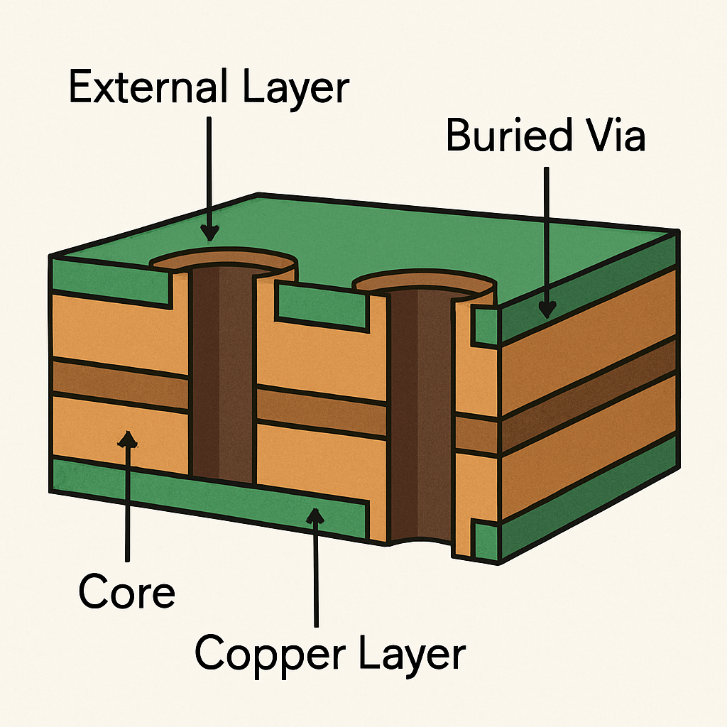
In PCB design, vias are small holes that facilitate electrical connections between different layers of the board, acting as conduits for electrical signals. Vias are typically classified into three types: through-hole, blind, and buried vias. Through-hole vias penetrate the entire board, connecting all layers from top to bottom. Blind vias connect the outer layer to one or more inner layers without traversing the entire board. Buried vias, in contrast, are completely encapsulated within the inner layers of the PCB, establishing connections without reaching the outer surfaces.
Buried vias are often employed in high-density interconnect (HDI) PCBs where space is at a premium. Their ability to create internal connections without occupying surface area is invaluable, particularly in designs requiring multiple layers of interconnections. This internalization not only saves space but also protects the vias from potential environmental damage, contributing to the reliability and longevity of the PCB.
Buried vias are pivotal in achieving higher density in PCB layouts. They allow designers to create more complex and compact multilayer boards without necessitating an increase in the overall size of the PCB. By eliminating the need for through-holes that span the entire board, buried vias help optimize the available surface area for placing components and routing traces. This optimization leads to enhanced performance and miniaturization of electronic devices, enabling more features to be packed into smaller form factors.
The significance of buried vias extends beyond mere space-saving. By facilitating efficient routing of electrical signals within the board, they contribute to improved signal integrity and reduced electromagnetic interference. This capability is particularly important in high-frequency applications where signal integrity is critical. Consequently, buried vias are not just a design convenience but a necessity in the pursuit of high-performance, miniaturized electronic devices.

The aspect ratio of a via refers to the ratio between its depth and its diameter. A 4:1 aspect ratio means that the depth of the via is four times its diameter. This high aspect ratio poses particular challenges in PCB manufacturing due to the precision required in drilling and plating processes. However, it is a critical factor in modern high-performance PCBs, as it allows for even more compact designs and efficient use of space.
High aspect ratio vias are essential for accommodating complex multilayer PCBs without increasing their footprint. The ability to maintain a 4:1 aspect ratio ensures that even with increased depth, the via does not occupy unnecessary space on the board's surface, allowing for more efficient layouts and routing. This efficiency is particularly beneficial in applications where space is limited, such as in handheld devices and compact electronic modules.
Space Efficiency: With a 4:1 aspect ratio, buried vias occupy less space, allowing for a denser arrangement of components and traces on the PCB. This efficiency supports the trend toward smaller and more powerful electronic devices, meeting consumer demand for compactness without sacrificing functionality.
Improved Signal Integrity: These vias minimize the path length for signals, which can reduce signal loss and improve overall signal integrity. By shortening the path signals must travel, buried vias help maintain the speed and clarity of data transmission, which is crucial in high-speed and high-frequency applications.
Enhanced Thermal Management: Efficient heat dissipation is crucial in high-performance electronics. Buried vias with high aspect ratios can help manage heat distribution more effectively, contributing to the longevity and reliability of the device. By facilitating internal heat transfer, these vias prevent hotspots and ensure uniform thermal distribution across the PCB.

Manufacturing PCBs with high aspect ratio buried vias requires precision drilling techniques. The challenge lies in creating vias that are deep yet narrow, maintaining the required aspect ratio without compromising the structural integrity of the PCB. Achieving this precision demands advanced equipment and techniques, as even slight deviations can affect the performance and reliability of the PCB.
Precision drilling is not only about accuracy but also about maintaining the consistency and quality of the vias across the entire board. This consistency is crucial for ensuring that all vias perform as expected, particularly in high-density PCBs where numerous vias are used. As such, manufacturers must implement rigorous quality control measures to guarantee the precision and reliability of the drilling process.
The plating process for high aspect ratio vias must ensure that the walls of the vias are adequately coated with conductive material to facilitate electrical connections. Additionally, the filling process must be carefully controlled to avoid voids or defects, which could impede the functionality of the PCB. This requires meticulous attention to detail and advanced techniques to ensure uniform plating and filling.
The challenges of plating and filling are compounded by the need to maintain the integrity of the high aspect ratio. Any inconsistencies in the plating thickness or filling material can lead to electrical failures or mechanical weaknesses. Therefore, manufacturers must employ state-of-the-art equipment and processes to achieve the desired quality and reliability in high aspect ratio vias.

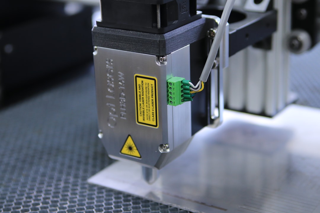
One of the significant advancements in manufacturing high aspect ratio vias is the adoption of laser drilling technology. Laser drills offer unparalleled precision, allowing manufacturers to create extremely small and accurate vias necessary for maintaining the 4:1 aspect ratio. This technology provides the accuracy needed to produce vias that meet the stringent requirements of modern PCB designs.
Laser drilling not only improves precision but also enhances the speed and efficiency of the manufacturing process. By reducing the time required for drilling and minimizing errors, laser technology contributes to faster production times and lower costs, making it an attractive option for manufacturers seeking to optimize their operations.
Innovations in plating techniques, such as copper pulse plating, have improved the reliability and quality of high aspect ratio vias. These techniques ensure even coating and filling of the vias, reducing the risk of failures in high-density PCBs. By providing consistent and uniform plating, these advanced techniques enhance the electrical and mechanical performance of the vias.
Advanced plating techniques also contribute to the overall durability and longevity of the PCB. By ensuring that the vias are properly coated and filled, these techniques prevent issues such as corrosion or mechanical failure, which can compromise the performance and reliability of the PCB in demanding applications.
New materials with better thermal and mechanical properties have been developed to support the manufacturing of high aspect ratio buried vias. These materials enhance the performance and durability of the PCB, making them suitable for advanced electronic applications. By offering improved thermal conductivity and mechanical strength, these materials support the reliable operation of high-performance devices.
Material innovations also play a critical role in addressing the challenges associated with high aspect ratio vias. By providing materials that can withstand the rigors of manufacturing and operational stresses, these innovations ensure that PCBs can meet the demanding requirements of modern electronics without compromising on performance or reliability.
In consumer electronics, such as smartphones and tablets, the demand for compact and powerful devices is ever-increasing. PCBs with 4:1 aspect ratio buried vias enable the integration of more features and functions into smaller form factors. This capability is essential for meeting consumer expectations for sleek, lightweight devices that offer advanced functionality and performance.
The use of high aspect ratio buried vias in consumer electronics also supports the development of next-generation devices with enhanced capabilities. By facilitating more complex designs, these vias allow manufacturers to incorporate new technologies and features that improve the user experience and meet the evolving demands of the market.
The automotive and aerospace industries require highly reliable and efficient electronic systems to operate in challenging environments. High aspect ratio buried vias contribute to the performance and reliability of these systems by allowing for compact and robust PCB designs. These designs are critical for ensuring the safe and efficient operation of vehicles and aircraft in demanding conditions.
In these industries, the ability to create compact and reliable electronic systems is essential for meeting stringent safety and performance standards. High aspect ratio buried vias support these requirements by providing the flexibility and reliability needed to develop cutting-edge technologies that enhance vehicle and aircraft performance.
In telecommunications, where high-speed data transmission is critical, PCBs with 4:1 aspect ratio buried vias help maintain signal integrity and reduce interference, leading to better performance of communication devices. By ensuring efficient signal routing and minimizing losses, these vias support the development of advanced telecommunications infrastructure capable of handling increased data loads.
The role of high aspect ratio buried vias in telecommunications extends beyond signal integrity. By enabling more compact and efficient designs, these vias support the deployment of advanced communication networks that offer faster speeds and greater reliability, meeting the growing demand for connectivity in today's digital world.
The use of 4:1 aspect ratio buried vias in PCB manufacturing is a testament to the industry's commitment to innovation and efficiency. As technology continues to advance, these high aspect ratio vias will play an increasingly vital role in the development of compact, high-performance electronic devices. By understanding the benefits and challenges associated with these vias, manufacturers and designers can better harness their potential to create the next generation of electronic products.
The ongoing advancements in materials, drilling, and plating technologies will further enhance the capabilities of high aspect ratio buried vias, driving innovation across various industries. As electronic devices become more complex and demanding, the importance of these vias in facilitating efficient and reliable designs will only continue to grow, cementing their place as a cornerstone of modern PCB technology.

Got project ready to assembly? Contact us: info@apollopcb.com


We're not around but we still want to hear from you! Leave us a note:

Leave Message to APOLLOPCB
