-
- PCB TYPE
- PRINTED CIRCUIT BOARD PROTOTYPE ALUMINUM PRINTED CIRCUIT BOARD R&F PCB FPC HIGH FREQUENCY PCB HIGH-TG PCB HEAVY COPPER PCB HDI PCB PCB FOR LIGHTING METAL CORE PCB
time:Jul 02. 2025, 15:22:11
The Evolutionary Leap in High-Density Interconnect Technology
In the ever-shrinking universe of advanced electronics, where devices must pack unprecedented power into palm-sized forms, a revolutionary pairing has emerged: Blind and Buried Vias (BBVs) in Aluminum High-Density Interconnect (HDI) PCBs. This technology represents a quantum leap beyond traditional through-hole vias, enabling engineers to create electronic marvels that blend extreme miniaturization with robust thermal management. Picture a world where smartphones host AI processors in spaces once occupied by simple chips, where medical implants monitor vital signs with nanoscale precision, and where aerospace systems withstand the harshest environments while shrinking in size—all made possible by the intricate dance of BBVs within aluminum HDI structures. This article delves into the technical wonders, manufacturing complexities, and transformative applications of this cutting-edge technology, illuminating how it’s reshaping the future of electronics.
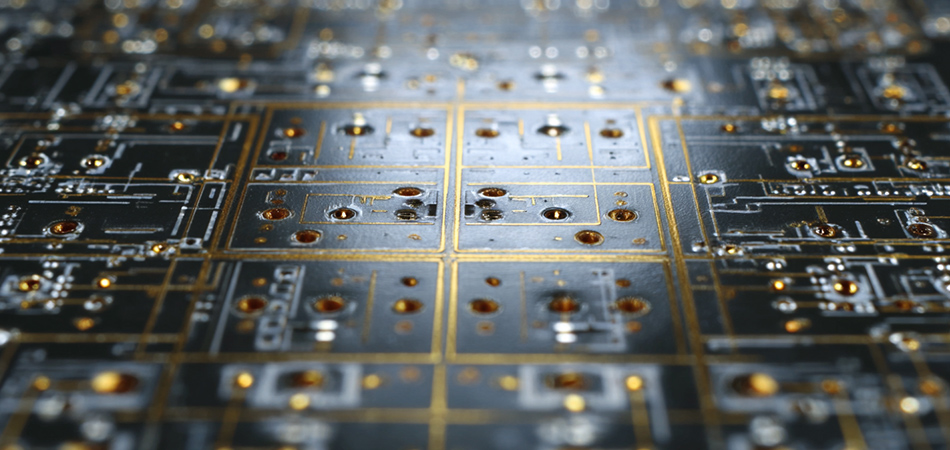
Technical Foundations: Redefining Connectivity in Three Dimensions
The Architecture of Miniaturization: BBVs vs. Traditional Vias
Blind and Buried Vias introduce a paradigm shift in PCB connectivity:
Blind Vias: These vias start on an outer layer and terminate within the board, like tunnels that open only on one side. They enable direct connections from surface-mounted components to internal layers without penetrating the entire board, reducing signal loss and improving routing density.
Buried Vias: Hidden entirely within the board’s layers, these vias connect internal traces without ever reaching the surface. They act as invisible bridges between inner circuitry, freeing up surface space for component placement and enhancing overall design efficiency.
Traditional Through-Hole Vias: In contrast, these vias penetrate the entire board, often leaving unused holes on the opposite surface. They consume more space, limit routing options, and can act as thermal and electrical bottlenecks in high-density designs.
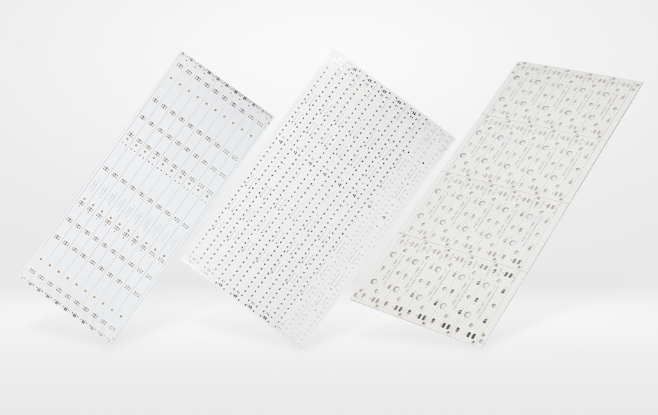
Aluminum HDI: A Symphony of Thermal Management and Density
Combining BBVs with aluminum HDI substrates creates a technical marvel:
Aluminum Substrate Advantage: The thermal conductivity of aluminum serves as a foundation for efficient heat dissipation, while its mechanical rigidity supports the thin, multi-layer structures required for HDI designs. It’s like building a skyscraper on a foundation that both withstands earthquakes and regulates temperature.
High-Density Interconnect Layers: HDI technology allows for finer traces, smaller pads, and higher component density. When paired with BBVs, it enables a 3D network of connections that would be impossible with traditional vias, much like constructing a city with multi-level highways to ease congestion.
Thermal-Via Synergy: BBVs can be specifically designed as thermal vias, creating vertical pathways that carry heat from power-dense components to the aluminum base. This is akin to building chimneys in a house to draw heat away from living spaces, ensuring no single area overheats.
Material Considerations for BBV Aluminum HDI PCBs
Dielectric Materials: Advanced thermally conductive dielectrics, often filled with nano-scale ceramic particles, are essential. These materials must balance electrical insulation with efficient heat transfer, acting as both a barrier and a conduit—imagine a window that blocks noise but lets sunlight pass.
Copper Foil Thickness: Ultra-thin copper foils (as thin as a human hair) are used to create fine traces, while maintaining electrical conductivity. This is similar to using lightweight yet strong cables in a high-performance audio system.
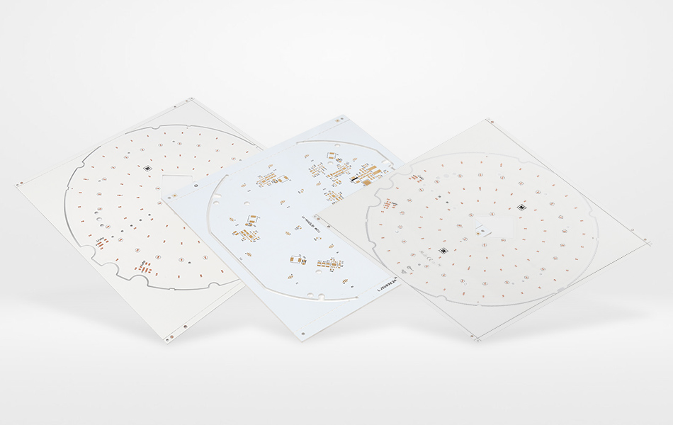
Manufacturing Processes: Crafting Microscopic Marvels with Precision
Layer Lamination: Building the Foundation
Prepreg Lamination: Thin layers of resin-impregnated glass fabric (prepreg) are sandwiched between copper foils and the aluminum substrate. This process, under high heat and pressure, bonds the layers together, creating a uniform base—think of it as layering ingredients in a cake, each step critical for the final structure.
Aluminum Substrate Treatment: The aluminum surface undergoes precise cleaning and roughening to ensure optimal adhesion with the dielectric layers. This is similar to sanding a piece of wood before painting, ensuring the finish sticks perfectly.
Via Formation: Drilling with Nanoscale Accuracy
Laser Drilling for Blind Vias: Ultraviolet (UV) or CO2 lasers are used to create blind vias with diameters as small as 50 microns. The laser acts like a precision scalpel, etching through the top layers to the desired depth without penetrating further—imagine a dentist using a laser to make a tiny cavity without hitting the nerve.
Mechanical Drilling for Buried Vias: For buried vias, specialized drills create holes in partial-layer stacks before lamination. These holes are then plated to form connections between internal layers, like building a tunnel between two underground chambers before constructing the ground above.
Via Bottom Detection: Advanced systems use optical or electrical feedback to ensure blind vias stop exactly at the target layer, preventing over-drilling that could damage underlying circuitry—similar to a 3D printer stopping at the precise height for each layer.
Electroless Plating: Creating Conductive Pathways
Via Plating Process: The drilled vias are coated with a thin layer of copper through an electroless plating process, turning insulating holes into conductive channels. This is like painting a tunnel with a conductive material to allow electricity to flow through.
Thickness Control: The copper plating thickness is carefully controlled to ensure uniform conductivity and mechanical strength, balancing the need for reliable connections with the constraints of miniaturization—much like building a bridge that’s strong enough to carry traffic but not too heavy for its foundations.
Surface Finishing and Testing: Ensuring Reliability
Lead-Free Surface Finishes: Processes like electroless nickel immersion gold (ENIG) or organic solderability preservatives (OSP) are applied to ensure solderability and corrosion resistance. This is the final protective layer, like a clear coat on a luxury car, preserving performance over time.
Comprehensive Testing Regimes:
AOI (Automated Optical Inspection): High-resolution cameras inspect vias and traces for microscopic defects, acting as vigilant quality control inspectors.
Thermal Cycling Tests: PCBs are subjected to extreme temperature changes to ensure vias maintain connectivity, simulating the harsh conditions of space or industrial environments.
Electrical Testing: Every via and trace is tested for continuity and insulation, ensuring the PCB functions flawlessly—like a doctor performing a full-body scan to check for any issues.
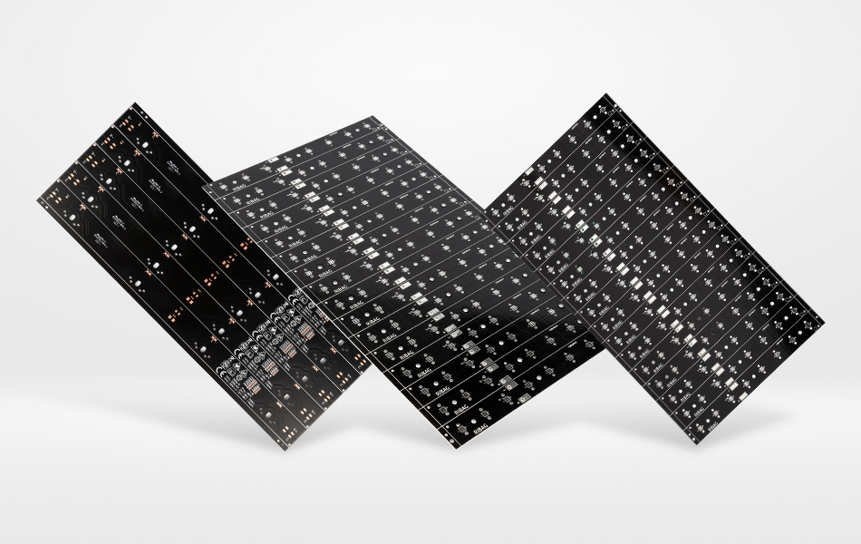
Performance Advantages: Miniaturization Meets Thermal Efficiency
Dense Connectivity Without Compromise
BBV Aluminum HDI PCBs enable a significant increase in component density:
Reduced Layer Count: By using BBVs, designers can achieve the same connectivity with fewer layers, shrinking the overall board size. It’s like building a city with subway systems that reduce the need for surface roads, freeing up space for buildings.
Fine-Pitch Component Support: The technology supports components with ultra-fine pitch (down to 0.3mm or less), allowing for the latest high-performance chips to be mounted—similar to fitting a supercomputer’s processing power into a laptop.
Superior Thermal Management
Targeted Heat Dissipation: BBVs can be strategically placed as thermal vias, directing heat from hot components to the aluminum substrate. This is like having a network of fans that only cool the areas that need it, improving efficiency.
Reduced Thermal Resistance: The combination of aluminum and BBVs creates a low-resistance thermal path, reducing hotspots and extending component lifespan—imagine a house with excellent insulation and ventilation that stays comfortable in any weather.
Improved Electrical Performance
Signal Integrity: Shorter signal paths and reduced via inductance in BBV designs improve high-frequency signal integrity, critical for 5G and IoT applications. It’s like having a direct, high-speed internet connection without lag.
EMI (Electromagnetic Interference) Reduction**: The compact, controlled via structures minimize electromagnetic radiation, making these PCBs ideal for sensitive medical and aerospace devices—similar to soundproofing a room to block external noise.
4Mechanical Robustness
Layer Bonding Strength: The lamination processes used in BBV Aluminum HDI PCBs create strong inter-layer bonds, resisting delamination even under thermal cycling—like a well-constructed puzzle where each piece fits tightly and stays together.
Flexibility in Design: Despite their complexity, these PCBs can be designed to be thin and lightweight, enabling portable device innovation—think of a high-performance sports car that’s both fast and agile.
Industry Applications: Transforming Technology Landscapes
5G and Advanced Communication Systems
Base Station Electronics: BBV Aluminum HDI PCBs enable the high-density, high-frequency circuitry required for 5G base stations, managing heat from multiple antennas and power amplifiers—like the control center of a bustling city, directing countless signals without confusion.
Mobile Devices: In smartphones and tablets, these PCBs support compact designs with powerful processors, ensuring smooth operation during data-intensive tasks—imagine a handheld device that can stream 4K video, play complex games, and run AI apps without overheating.
Medical and Healthcare Innovations
Implantable Devices: Ultra-thin BBV Aluminum HDI PCBs are ideal for medical implants, combining miniaturization with reliable thermal management—like a tiny computer inside the body that monitors vital signs and delivers treatments, all without overheating.
Diagnostic Equipment: High-precision PCBs for MRI and CT scanners, where signal integrity and thermal stability are critical for accurate imaging—similar to a microscope that can see the smallest details without distortion.
Aerospace and Defense Technologies
Satellite Electronics: BBV Aluminum HDI PCBs withstand the extreme temperatures and radiation of space, while enabling miniaturized satellite designs—like a spacecraft that’s both compact and robust enough for deep-space missions.
Military Electronics: Ruggedized PCBs for combat systems, ensuring reliable operation in harsh environments with vibration, temperature swings, and electromagnetic interference—think of a field radio that works perfectly in the desert or the arctic.
Automotive Electronics
Electric Vehicle (EV) Control Systems: These PCBs manage the high power and heat from EV batteries and motors, supporting compact, efficient designs—like the brain of an electric car that ensures the battery charges quickly and safely.
Advanced Driver Assistance Systems (ADAS): High-density PCBs for ADAS sensors and processors, enabling features like autonomous driving—similar to a car that can “see” and “think” faster than a human, thanks to its advanced electronic “nervous system.”
Consumer Electronics and IoT
Wearable Devices: Ultra-thin BBV Aluminum HDI PCBs for smartwatches and fitness trackers, combining multiple functions in a small package—like a wristwatch that can monitor your heart rate, track your movements, and even make calls.
Smart Home Sensors: Compact PCBs for IoT sensors that monitor everything from temperature to air quality, designed to be energy-efficient and long-lasting—imagine tiny devices throughout your home that work silently to make your life more comfortable and efficient.
Technological Trends and Innovations
Advanced Material Frontiers
Graphene-Enhanced Dielectrics: Research into dielectrics infused with graphene nanosheets promises even better thermal conductivity, like adding superhighways to an already efficient heat transport system.
Biodegradable Bonding Materials: Development of eco-friendly adhesives for layer lamination, reducing environmental impact—similar to using recycled paper instead of virgin materials.
Composite Aluminum Substrates: Combining aluminum with ceramics or carbon fibers to create substrates with tailored thermal and mechanical properties, like a custom-made tool designed for a specific task.
Manufacturing Process Innovations
Atomic Layer Deposition (ALD) for Vias: Ultra-thin, uniform copper plating using ALD, improving via reliability and reducing voids—like painting a tunnel with an extremely precise and even coat.
3D Laser Drilling: Multi-axis laser systems that can create angled or curved vias, enabling more complex 3D circuit routing—imagine building highways that curve and twist to fit through tight spaces.
AI-Driven Process Optimization**: Machine learning algorithms that predict and prevent manufacturing defects, like having a team of experts constantly analyzing data to improve quality.
Integration with Emerging Technologies
AI Chips and Edge Computing: BBV Aluminum HDI PCBs for next-generation AI processors, managing the intense heat from thousands of parallel computing cores—like a cooling system for a supercomputer that fits on a desk.
Quantum Computing Prototypes: High-precision PCBs for quantum bit (qubit) control systems, where thermal stability and signal integrity are paramount—similar to the delicate infrastructure needed to maintain quantum states.
Augmented Reality (AR) and Virtual Reality (VR): Compact, high-performance PCBs for AR/VR headsets, enabling immersive experiences without device overheating—like a pair of glasses that transport you to another world, comfortable to wear for hours.
Challenges and Mitigation Strategies
Extreme Miniaturization Complexity
Challenge: As vias and traces shrink, manufacturing precision becomes extremely difficult, like trying to paint a detailed picture on a grain of rice.
Mitigation: Investing in advanced laser systems and AI-driven quality control, like using a microscope and computer to ensure every detail is perfect.
Thermal Stress Management
Challenge: Different materials in the PCB expand and contract at different rates, leading to stress that can crack vias—imagine a bridge made of different metals that expand in the sun, causing cracks.
Mitigation: Careful material selection and design, like using metals that expand similarly, and adding stress-relieving features to the PCB design.
Cost of Advanced Manufacturing
Challenge: BBV Aluminum HDI PCB production is more expensive than traditional PCBs, like a luxury car costing more than a standard model.
Mitigation: Economies of scale and process optimization, like building more units to reduce the cost per PCB, and finding ways to make the manufacturing process more efficient.
Design Expertise Gap
Challenge: Designing BBV Aluminum HDI PCBs requires specialized knowledge, like building a skyscraper vs. a house.
Mitigation: Training programs and collaboration between PCB manufacturers and design houses, like schools teaching architects how to design tall buildings.
Future Outlook: BBV Aluminum HDI PCBs as Technology Enablers
As electronics continue their march toward ever-smaller, more powerful designs, Blind and Buried Vias in Aluminum HDI PCBs will be the cornerstone of innovation. They will enable technologies that were once the stuff of science fiction: foldable smartphones that don’t overheat, medical implants that last a lifetime, and autonomous vehicles that navigate complex environments with ease.
Manufacturers who master the art and science of BBV Aluminum HDI PCB production will lead the next wave of technological advancement. For engineers and designers, these PCBs are not just components but canvases for creating the future.
In the end, BBV Aluminum HDI PCBs are more than just pieces of technology; they are the enablers of a connected, intelligent, and miniaturized world. They work silently in the background, ensuring that our devices are powerful, reliable, and efficient—all while shrinking in size. As we move forward, these microscopic marvels will continue to push the boundaries of what’s possible, making the impossible possible, one via at a time.

Got project ready to assembly? Contact us: info@apollopcb.com


We're not around but we still want to hear from you! Leave us a note:

Leave Message to APOLLOPCB
