-
- PCB TYPE
- PRINTED CIRCUIT BOARD PROTOTYPE ALUMINUM PRINTED CIRCUIT BOARD R&F PCB FPC HIGH FREQUENCY PCB HIGH-TG PCB HEAVY COPPER PCB HDI PCB PCB FOR LIGHTING METAL CORE PCB
time:Aug 25. 2025, 17:37:19
CEM3 PCB has emerged as a critical enabler of distributed electronics networks—decentralized systems where sensors, controllers, and communication nodes work in tandem across large areas, from smart city infrastructure to agricultural fields. Unlike high-cost substrates that limit scalability or low-performance alternatives that fail in real-world conditions, CEM3 PCB balances three essential attributes for distributed systems: cost-effectiveness (enabling mass deployment), reliability (withstanding variable environmental conditions), and compatibility (supporting low-power, low-cost components).
Distributed electronics demand substrates that can be produced at scale without sacrificing quality—whether deploying 10,000 soil moisture sensors in a farm or 5,000 traffic monitoring nodes in a city. CEM3 PCB meets this need by retaining the mechanical and electrical stability required for long-term outdoor operation while remaining affordable enough to justify large-scale rollouts. This article explores how CEM3 PCB supports the unique requirements of distributed networks, its role in key decentralized applications, strategies for optimizing it for wide-area deployment, and how it aligns with trends like low-power IoT and edge computing. By focusing on “scalability for distributed systems,” it delivers a fresh perspective distinct from prior discussions of CEM3’s material properties or niche use cases, ensuring relevance for engineers, urban planners, and agricultural technologists building the next generation of interconnected infrastructure.
Distributed electronics networks—such as smart city sensor grids, precision agriculture systems, or industrial IoT (IIoT) deployments—face three core challenges that CEM3 PCB is uniquely positioned to solve:
Distributed networks often require thousands or tens of thousands of nodes. For example, a mid-sized city’s smart streetlight system may need 2,000+ control nodes, while a 1,000-acre farm could require 500+ soil sensors. CEM3 PCB’s cost structure makes such scale feasible:
Low Per-Unit Costs: CEM3 PCB costs 30–50% less than FR4 and 70–80% less than flexible PCBs (FPCs). For a farm deploying 500 sensors, using CEM3 instead of FR4 reduces PCB costs by \(1,500–\)2,500—a significant saving for budget-constrained agricultural tech projects.
High Production Yields: CEM3’s simple manufacturing process (compared to specialty substrates) achieves yield rates of 95%+ in high-volume production. This minimizes scrap and ensures consistent supply, critical for meeting tight deployment timelines (e.g., installing smart sensors before a planting season).
Distributed nodes operate outdoors or in unregulated environments—exposed to temperature swings, moisture, dust, and UV radiation. CEM3 PCB’s inherent properties address these challenges:
Temperature Tolerance: CEM3’s epoxy resin and glass fiber reinforcement retain stability across -30°C to 100°C, covering the operating range of most distributed applications (e.g., a smart city sensor in a desert climate or a farm sensor in a temperate region).
Moisture Resistance: Unlike paper-based CEM1, CEM3’s glass fiber core resists water absorption, preventing short circuits in rainy or humid conditions. This resilience extends node lifespan to 5–7 years, reducing maintenance costs for remote networks.
UV and Chemical Resistance: CEM3’s resin is formulated to resist UV degradation (critical for outdoor nodes exposed to sunlight) and mild chemicals (e.g., fertilizers in agricultural settings or road salts in smart city deployments).
Distributed nodes rely on low-power components (e.g., microcontrollers, wireless transceivers) to maximize battery life (often 2–5 years). CEM3 PCB’s design supports these components seamlessly:
Low-Power Circuitry: CEM3’s stable dielectric properties (low dissipation factor) minimize power loss in low-voltage circuits, ensuring efficient energy use. This is critical for battery-powered sensors that operate on 3.3V–5V.
Compatibility with Wireless Modules: CEM3 PCB’s flat, stable surface supports compact wireless modules (e.g., LoRa, Zigbee) used for long-range communication in distributed networks. Its dimensional stability ensures the modules remain aligned, preventing signal loss.
Mixed Component Support: Distributed nodes often combine through-hole components (e.g., batteries, connectors) with surface-mount devices (e.g., microchips). CEM3 PCB supports both, eliminating the need for separate substrates and simplifying node design.
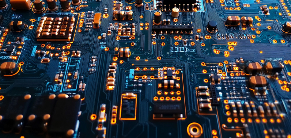
CEM3 PCB’s ability to balance scalability, resilience, and compatibility makes it indispensable in three high-impact distributed systems: smart cities, precision agriculture, and industrial IoT. Below is how it enables each application, with specific use cases and performance benefits.
Smart cities deploy distributed nodes to monitor traffic, manage energy, and improve public services. CEM3 PCB supports these networks by:
Enabling Compact, Low-Power Nodes: CEM3’s thin profile (down to 0.8mm) allows nodes to be integrated into existing infrastructure—e.g., traffic light controllers, streetlight sensors, or waste bin level monitors—without requiring major modifications.
Withstanding Urban Stressors: In city environments, nodes face vibration (from traffic), temperature swings (day/night cycles), and exposure to road salts or pollutants. CEM3’s mechanical resilience and chemical resistance ensure reliable operation, reducing maintenance calls.
Supporting Interoperability: Smart city nodes use diverse communication protocols (e.g., 5G, LoRaWAN). CEM3’s stable electrical properties maintain signal integrity across these protocols, ensuring nodes can communicate with central management systems.
Key Use Case: Smart Traffic Monitoring Nodes
These nodes, mounted on street poles or traffic lights, use cameras and motion sensors to track vehicle and pedestrian flow. CEM3 PCB’s compact design fits into small enclosures, while its temperature tolerance ensures reliable operation in summer heat (up to 40°C) and winter cold (down to -10°C). Its compatibility with low-power microcontrollers extends battery life to 3 years, reducing the need for frequent maintenance in busy urban areas.
Precision agriculture uses distributed sensors to monitor soil moisture, temperature, and crop health, optimizing water and fertilizer use. CEM3 PCB supports these systems by:
Resisting Agricultural Environments: Farm sensors are exposed to rain, humidity, fertilizers, and pests. CEM3’s moisture resistance prevents short circuits, while its chemical resistance withstands fertilizer runoff.
Enabling Low-Cost Sensor Networks: A 1,000-acre farm may need 500+ soil moisture sensors. CEM3’s low cost (\(2–\)3 per sensor PCB) makes this scale feasible, unlike FR4 (\(5–\)7 per PCB) or ceramic (\(15–\)20 per PCB) substrates.
Supporting Solar-Powered Nodes: Many farm sensors use small solar panels for power. CEM3’s compatibility with low-voltage solar regulators ensures efficient energy conversion, extending node operation even in cloudy conditions.
Key Use Case: Soil Moisture and Temperature Sensors
These sensors are buried or mounted near crops to transmit real-time data to irrigation systems. CEM3 PCB’s moisture resistance prevents water damage, while its stability across -10°C (winter) to 50°C (summer) ensures accurate readings year-round. Its low power consumption allows the sensors to run on a small battery or solar panel for 4–5 years.
Manufacturers use distributed IIoT nodes to monitor equipment health, track inventory, and optimize production across multiple facilities. CEM3 PCB supports these networks by:
Withstanding Industrial Stressors: Factory nodes face vibration (from machinery), dust, and oil exposure. CEM3’s dense glass fiber layers resist dust ingress, while its chemical resistance repels industrial oils, ensuring reliable operation in manufacturing environments.
Enabling Real-Time Data Transmission: IIoT nodes require stable signal integrity for real-time monitoring (e.g., tracking conveyor belt speed). CEM3’s low signal loss ensures data is transmitted accurately to central control systems, preventing production delays.
Scaling Across Multiple Facilities: A manufacturer with 5 factories may need 1,000+ IIoT nodes. CEM3’s high production yields and low cost enable consistent deployment across all facilities, simplifying supply chain management.
Key Use Case: Predictive Maintenance Sensors
These nodes are attached to machinery (e.g., motors, pumps) to monitor vibration, temperature, and pressure—alerting maintenance teams to potential failures. CEM3’s vibration resistance prevents sensor damage, while its temperature stability ensures accurate readings in factory environments (20°C–80°C). Its compatibility with wireless transceivers allows data to be sent to a central dashboard, enabling proactive maintenance.
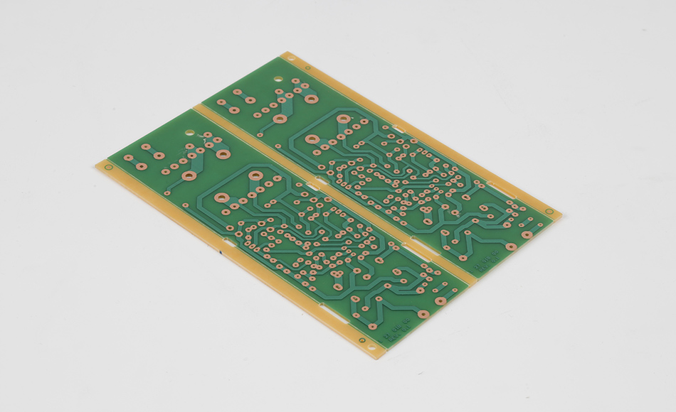
While CEM3 PCB is inherently suited for distributed networks, optimizing its design for specific deployment scenarios ensures maximum performance and longevity. Below are actionable strategies for engineers building distributed nodes.
Conformal Coating: Apply a thin, UV-resistant conformal coating (e.g., acrylic or silicone) to the PCB to protect against moisture, dust, and UV radiation. Silicone coatings are ideal for extreme temperatures (-40°C to 150°C), while acrylic coatings are cost-effective for milder climates.
Sealed Enclosures: Pair CEM3 PCB with IP67 or IP68-rated enclosures to prevent water and dust ingress. Ensure the enclosure has adequate ventilation to prevent heat buildup, as CEM3’s performance degrades above 100°C.
Corrosion-Resistant Components: Use components with corrosion-resistant finishes (e.g., gold-plated connectors) to complement CEM3’s chemical resistance. This is critical for nodes exposed to road salts (smart cities) or fertilizers (agriculture).
Minimize Power Loss: Use narrow, high-purity copper traces (0.1–0.2mm) to reduce resistance and power consumption. CEM3’s stable dielectric properties ensure these traces maintain signal integrity despite their small size.
Optimize Component Placement: Group low-power components (e.g., microcontrollers, sensors) near the battery to minimize voltage drop. Avoid placing high-power components (e.g., wireless transceivers) next to sensitive sensors, as this can cause interference and increase power use.
Sleep Mode Support: Design the PCB to support component sleep modes (common in low-power IoT devices). CEM3’s stable electrical properties ensure components wake reliably from sleep, reducing unnecessary power drain.
Standardize PCB Design: Use a single CEM3 PCB design for all nodes in a network, even if some nodes have additional components (e.g., a solar panel connector). This reduces manufacturing complexity and allows for easy upgrades.
Modular Connector Design: Incorporate standard modular connectors (e.g., USB-C, JST) to simplify installation and maintenance. CEM3’s mechanical stability ensures connectors remain secure, even in remote locations.
Batch Testing: Test CEM3 PCBs in batches of 100–500 to ensure consistency before mass deployment. Focus on key metrics like insulation resistance (to check moisture resistance) and signal integrity (to verify communication performance).
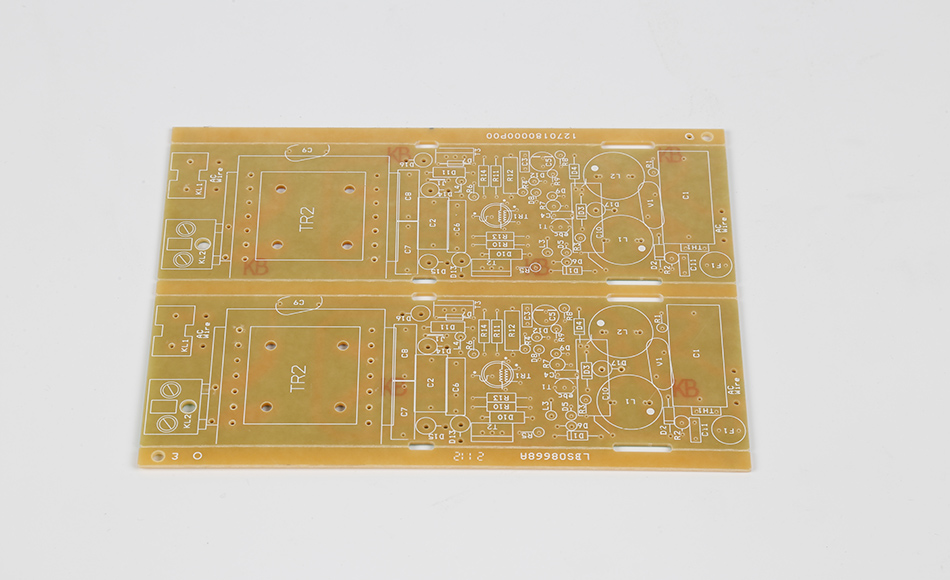
Distributed electronics networks cannot tolerate frequent failures—especially in remote locations where maintenance is costly. To ensure CEM3 PCB meets the demands of these systems, manufacturers and engineers must conduct targeted quality tests focused on scalability, resilience, and long-term performance.
Production Yield Validation: Test 1,000+ CEM3 PCBs to verify yield rates (target: ≥95%). Low yields indicate manufacturing inconsistencies that will increase costs in large-scale deployments.
Cost-Efficiency Audit: Calculate the total cost per PCB (including materials, manufacturing, and testing) to ensure it aligns with budget targets for mass deployment. CEM3 should cost 30–50% less than FR4 in high-volume production.
Temperature Cycling: Expose CEM3 PCBs to -30°C to 100°C for 1,000 cycles (per IEC 60068-2-14). The PCB must retain electrical continuity and mechanical strength, with no delamination or trace damage.
Moisture Resistance: Test PCBs at 85°C/85% RH for 1,000 hours (per IEC 60068-2-38). Insulation resistance must remain above 100 MΩ at 500V DC to prevent short circuits in humid conditions.
UV Exposure: Expose PCBs to UV radiation (simulating 5 years of outdoor sunlight) per ASTM G154. The resin should show no cracking or discoloration, and electrical performance must remain stable.
Life Cycle Simulation: Test CEM3 PCBs under simulated operating conditions (e.g., low-power mode, periodic wireless transmission) for 5,000 hours. This validates that the PCB will support node operation for 4–5 years without failure.
Vibration Testing: Subject PCBs to sinusoidal vibration (10–2,000 Hz) for 100 hours (per IEC 60068-2-6). This simulates vibration from traffic (smart cities) or machinery (IIoT), ensuring solder joints and components remain secure.
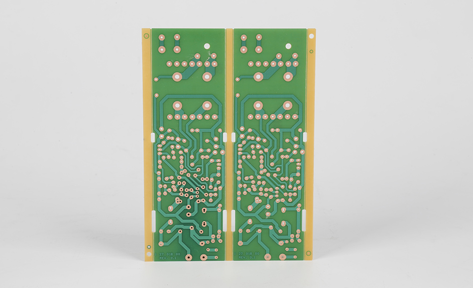
CEM3 PCB’s balance of scalability, resilience, and cost makes it superior to alternatives for most distributed electronics applications. Below is how it compares to common substrates:
Cost: FR4 costs 40–60% more than CEM3 in high-volume production, making it impractical for 1,000+ node deployments.
Resilience: FR4 offers slightly higher temperature resistance but is less flexible, making it harder to integrate into compact or irregularly shaped enclosures (e.g., streetlight sensors).
Use Case: FR4 for high-power industrial nodes (e.g., factory controllers), CEM3 for low-power distributed sensors (e.g., smart city traffic nodes).
Cost: FPCs cost 3–5x more than CEM3 and have lower production yields (80–85%), limiting scalability.
Resilience: FPCs are more flexible but prone to creasing and moisture damage, making them unsuitable for outdoor distributed nodes.
Use Case: FPCs for wearable devices, CEM3 for fixed outdoor nodes (e.g., agricultural sensors).
Resilience: CEM1 absorbs moisture and degrades in UV light, with a lifespan of 1–2 years—far shorter than CEM3’s 5–7 years.
Cost: CEM1 is slightly cheaper than CEM3 but requires more frequent replacement, increasing long-term maintenance costs for distributed networks.
Use Case: CEM1 for disposable electronics (e.g., temporary event sensors), CEM3 for permanent distributed nodes.
Cost: Ceramic substrates cost 10–15x more than CEM3, making them impossible to scale for 100+ node deployments.
Resilience: Ceramics offer superior temperature resistance but are brittle, making them prone to damage during installation or in vibration-prone environments.
Use Case: Ceramics for high-temperature industrial sensors (e.g., furnace monitors), CEM3 for most distributed applications.
Future Trends: CEM3 PCB Evolving for Next-Gen Distributed Networks
As distributed electronics become more advanced—with higher connectivity, longer battery life, and greater sustainability—CEM3 PCB is evolving to meet these demands:
1. Integration with Energy Harvesting
Future distributed nodes will rely on energy harvesting (e.g., solar, vibration, or RF energy) to eliminate batteries. CEM3 PCB is being optimized for this by:
Supporting Thin-Film Solar Panels: CEM3’s flat, stable surface allows direct integration of thin-film solar cells, reducing node size and weight.
Enhancing Thermal Conductivity: Adding thermally conductive fillers to CEM3’s resin improves heat dissipation for nodes using thermal energy harvesting (converting heat to electricity).
2. Sustainable Materials for Green Networks
To align with global sustainability goals (e.g., the EU’s Green Deal), manufacturers are developing eco-friendly CEM3 variants:
Recycled Glass Fibers: Using recycled glass fibers reduces reliance on virgin resources, lowering CEM3’s carbon footprint by 20–25%.
Bio-Based Epoxy Resins: Epoxy resins derived from plant oils (e.g., castor oil) replace petroleum-based resins, maintaining performance while reducing environmental impact.
3. 5G and Low-Orbit Satellite Compatibility
Next-gen distributed networks will use 5G and low-orbit satellites for long-range, high-speed communication. CEM3 PCB is being optimized for this by:
Improving High-Frequency Performance: Modifying CEM3’s resin to reduce signal loss at 5G frequencies (2–6 GHz), ensuring reliable communication in smart city and agricultural networks.
Enhancing Radiation Resistance: Adding radiation-shielding additives to CEM3’s resin for nodes in high-altitude or satellite-connected networks (e.g., weather monitoring nodes).
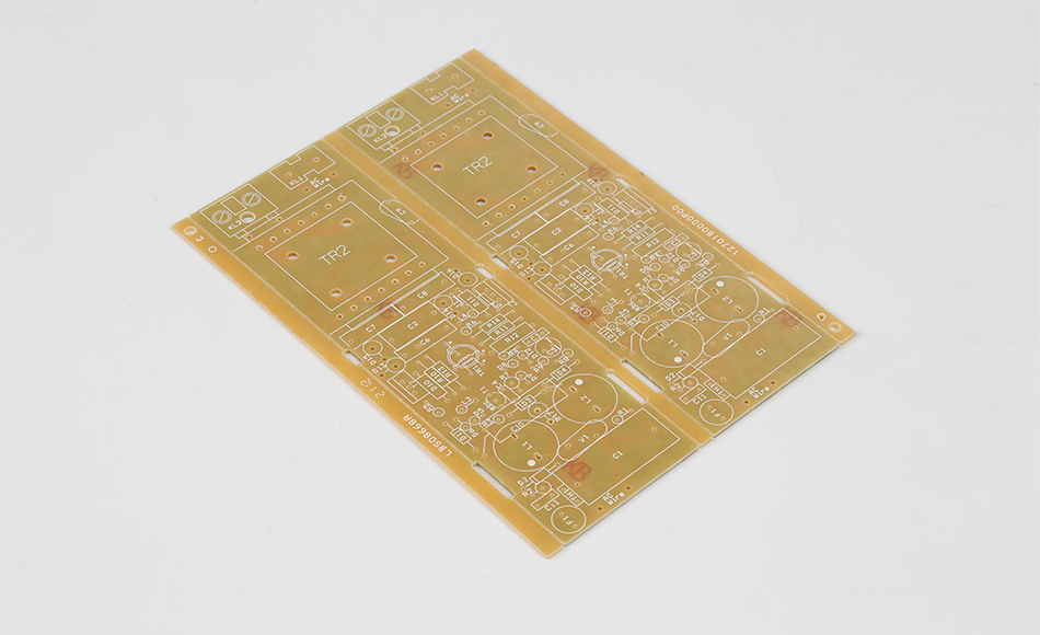
CEM3 PCB is the unsung hero of distributed electronics networks, enabling the scalable, reliable, and cost-effective deployment of smart city, agricultural, and industrial IoT systems. Its unique balance of affordability, environmental resilience, and component compatibility addresses the core challenges of decentralized electronics—challenges that high-cost or low-performance substrates cannot solve.
As the world becomes more interconnected, the demand for distributed networks will only grow. CEM3 PCB will remain at the forefront of this growth, evolving to support energy harvesting, sustainable manufacturing, and next-gen communication protocols. For engineers, planners, and technologists building the future of interconnected infrastructure, CEM3 PCB represents a strategic choice: a substrate that delivers the scalability and reliability needed to turn large-scale distributed visions into reality—one node at a time.

Got project ready to assembly? Contact us: info@apollopcb.com


We're not around but we still want to hear from you! Leave us a note:

Leave Message to APOLLOPCB
