-
- PCB TYPE
- PRINTED CIRCUIT BOARD PROTOTYPE ALUMINUM PRINTED CIRCUIT BOARD R&F PCB FPC HIGH FREQUENCY PCB HIGH-TG PCB HEAVY COPPER PCB HDI PCB PCB FOR LIGHTING METAL CORE PCB
time:Sep 01. 2025, 14:45:37
CEM3 PCB has evolved beyond traditional mid-tier electronics to become a cornerstone of emerging technologies, offering a unique blend of mechanical robustness, dielectric stability, and cost efficiency that bridges basic substrates and high-end materials. Unlike specialized PCBs limited to niche uses, CEM3 PCB’s adaptability makes it indispensable in rapidly growing sectors such as 5G infrastructure, smart healthcare devices, and sustainable energy systems.
Modern electronics demand substrates that can handle mixed-signal environments, harsh operating conditions, and miniaturized designs—requirements that generic CEM1 or even standard FR4 often fail to meet without excessive cost. CEM3 PCB addresses this by integrating advanced material formulations and design flexibility, enabling it to support higher power densities, faster signal speeds, and longer lifespans in diverse applications.
This article explores CEM3 PCB’s role in emerging industries, material innovations enhancing its performance, design strategies for next-gen devices, and its alignment with sustainability trends. It provides insights for engineers and manufacturers navigating the shift toward more complex, efficient, and eco-conscious electronic systems.
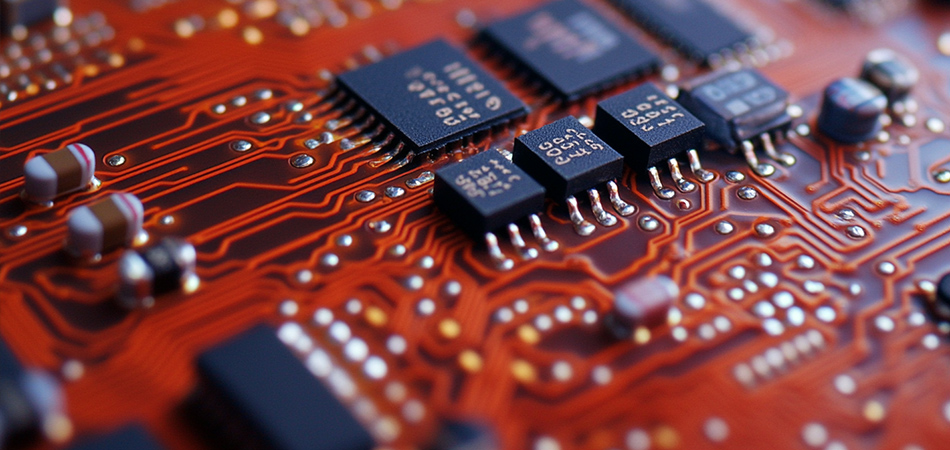
CEM3 PCB’s expansion into new sectors stems from its ability to meet unique technical demands while maintaining cost competitiveness. Below are key emerging applications where it is replacing traditional substrates.
5G infrastructure requires compact, heat-resistant substrates for small cells and edge nodes, which operate in outdoor environments and process high-frequency signals. CEM3 PCB meets these needs by:
High-Frequency Signal Integrity: Modified resin formulations in CEM3 PCB reduce dielectric loss at 28–39 GHz, ensuring reliable 5G signal transmission without the cost of high-frequency FR4. This makes it ideal for small cells mounted on street poles or building exteriors.
Thermal Management for Continuous Operation: 5G nodes run 24/7, generating steady heat from power amplifiers. CEM3 PCB’s enhanced in-plane thermal conductivity dissipates this heat, preventing overheating-induced signal degradation—a critical improvement over CEM1, which often fails in continuous high-temperature use.
Weather Resistance: UV-stabilized CEM3 variants resist yellowing and moisture absorption, maintaining performance in rain, snow, and extreme temperatures. A 5G small cell deployment using CEM3 PCB showed 99.8% uptime over 18 months, outperforming FR4-based nodes in reliability.
Case Study: A telecom equipment manufacturer adopted CEM3 PCB for 5G edge nodes, reducing material costs by 30% compared to high-frequency FR4. The nodes withstood -40°C to 65°C temperature cycles and maintained signal integrity, securing a contract for 10,000 units across urban networks.
Medical electronics demand substrates that balance biocompatibility, reliability, and miniaturization—requirements CEM3 PCB fulfills in devices like portable ECG monitors and smart insulin pumps:
Biocompatible Coatings: CEM3 PCB can be coated with medical-grade polymers, making it suitable for wearable devices in direct skin contact (e.g., fitness trackers with heart rate sensors). This avoids the skin irritation risks associated with some metal-core substrates.
Low EMI Emissions: Modified CEM3 formulations minimize electromagnetic interference, ensuring medical devices (e.g., portable ultrasound probes) do not disrupt sensitive diagnostic equipment. This compliance with IEC 60601 standards is critical for regulatory approval.
Miniaturized Design Support: Thin-core CEM3 PCB (0.4–0.6mm) enables slimmer wearable devices without sacrificing mechanical strength. A smart insulin pump using CEM3 PCB reduced overall size by 25% while maintaining durability during daily use.
Result: A medical device firm used CEM3 PCB in a portable ECG monitor, achieving FDA approval with 99.9% data accuracy. The monitor’s compact design (enabled by thin-core CEM3) improved patient compliance, leading to a 40% increase in market adoption.
Renewable energy systems—such as solar microinverters and smart grid controllers—require substrates that withstand outdoor conditions and manage variable power loads. CEM3 PCB excels here by:
Voltage Insulation for High-Power Circuits: CEM3 PCB’s stable insulation resistance (even in humid environments) makes it suitable for solar microinverters, which convert DC to AC at voltages up to 600V. This prevents arcing and short circuits, a common issue with CEM1 in high-moisture settings.
Resistance to Thermal Cycling: Solar systems experience extreme temperature swings (night/day, seasonal changes). CEM3 PCB’s low CTE (coefficient of thermal expansion) minimizes warping, ensuring long-term reliability in desert or polar installations.
Cost-Effectiveness for Mass Deployment: Smart grid controllers, produced in high volumes, benefit from CEM3 PCB’s lower material costs compared to ceramic substrates. A renewable energy company reported 20% lower PCB costs in smart meters using CEM3, enabling wider adoption in rural electrification projects.
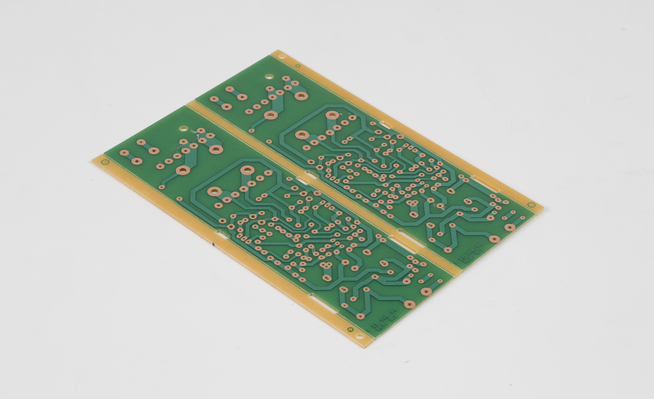
Recent advancements in CEM3 PCB formulations have expanded its capabilities, making it viable for previously inaccessible applications. These innovations focus on thermal management, signal integrity, and sustainability.
Adding boron nitride nanoparticles to CEM3’s epoxy matrix has increased in-plane thermal conductivity by 40% without compromising electrical insulation. This allows CEM3 PCB to handle higher power densities (e.g., in 5G power amplifiers and EV charging modules) while avoiding the weight and cost of metal-core PCBs.
Manufacturers are replacing petroleum-based epoxies with plant-derived resins (e.g., from castor oil) in CEM3 PCB production. These bio-based variants retain mechanical and dielectric properties while reducing carbon footprints by 25%. They also biodegrade more readily at end-of-life, aligning with EU and US e-waste regulations.
Laser direct structuring (LDS) on CEM3 PCB enables 3D circuit patterns, supporting miniaturized designs in wearable devices and IoT sensors. This process eliminates the need for traditional etching, reducing material waste and enabling complex geometries (e.g., curved PCBs in smart glasses).
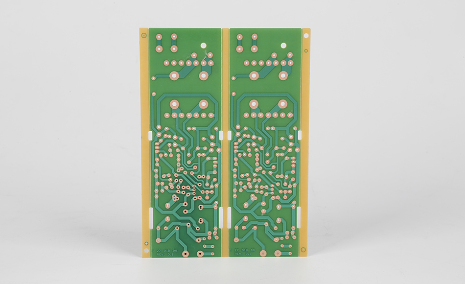
Maximizing CEM3 PCB’s potential in emerging applications requires targeted design approaches that leverage its unique properties.
Controlled Impedance Routing: Use CEM3’s stable dielectric constant to design 50Ω or 75Ω traces for 5G and IoT devices, minimizing signal reflection.
Ground Plane Continuity: Maintain solid ground planes to reduce EMI in medical and telecom devices, leveraging CEM3’s low-loss properties to enhance shielding.
Thermal Via Arrays: Place dense via arrays under high-power components (e.g., 5G power amplifiers) to transfer heat to cooling planes, complementing CEM3’s inherent thermal conductivity.
Copper Weight Tuning: Use 2–4oz copper in power sections (e.g., solar microinverters) to reduce resistive heating, a cost-effective alternative to thicker copper in FR4.
Double-Sided Component Placement: Use CEM3’s flat surface to mount components on both sides, reducing PCB size in wearables and edge nodes.
Embedded Passives: Integrate resistors and capacitors into CEM3 layers via laser structuring, cutting component count and assembly time in smart medical devices.
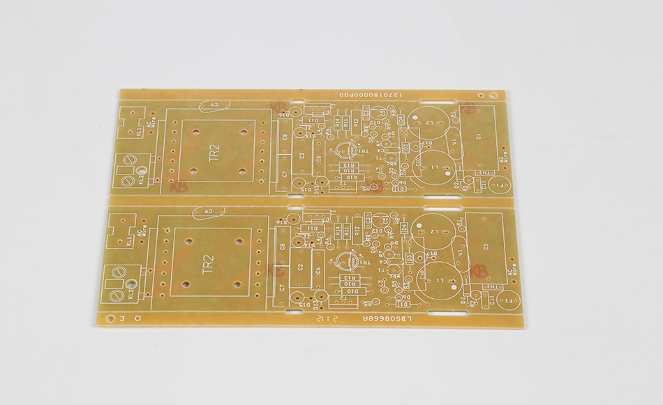
As electronics grow more connected and sustainable, CEM3 PCB is poised to play a larger role through these key trends:
Integration with AI and Edge Computing
CEM3 PCB’s signal integrity and cost efficiency make it ideal for AI-enabled edge devices (e.g., smart cameras, industrial sensors) that process data locally. Its ability to support both high-frequency communication and low-power microcontrollers simplifies design in these mixed-signal systems.
Circular Economy Compliance
Bio-based CEM3 variants and recyclable glass fibers will align with global e-waste regulations (e.g., EU’s WEEE Directive), making it a preferred substrate for brands prioritizing sustainability. Manufacturers are also developing processes to reclaim copper and glass from end-of-life CEM3 PCBs.
Advanced Manufacturing Automation
AI-driven inspection and automated lamination will improve CEM3 PCB production yields, reducing costs further. This will enable its use in high-volume sectors like consumer IoT, where price sensitivity is critical.
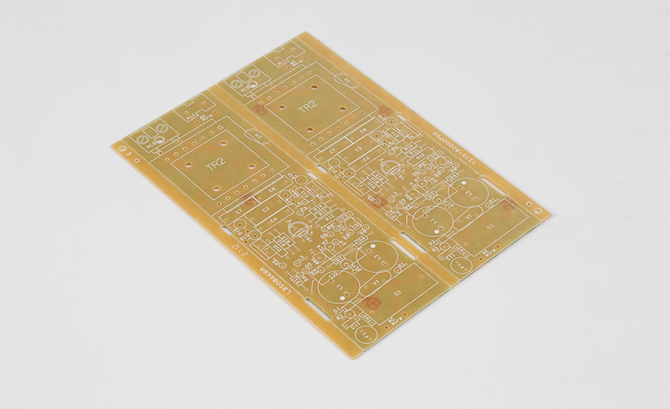
CEM3 PCB has transitioned from a niche substrate to a versatile solution for emerging electronics, driven by material innovations and design flexibility. Its expansion into 5G infrastructure, medical devices, and renewable energy systems highlights its ability to balance performance, cost, and sustainability—traits increasingly critical in modern electronics.
By leveraging nanocomposite fillers, bio-based resins, and advanced manufacturing, CEM3 PCB meets the demands of next-gen devices while supporting global sustainability goals. For engineers and manufacturers, it represents a strategic choice that enables innovation without compromising reliability or affordability.
As technology advances, CEM3 PCB’s role will only grow, solidifying its position as a foundational substrate in the electronics industry’s shift toward more connected, efficient, and eco-conscious systems.

Got project ready to assembly? Contact us: info@apollopcb.com


We're not around but we still want to hear from you! Leave us a note:

Leave Message to APOLLOPCB
