-
- PCB TYPE
- PRINTED CIRCUIT BOARD PROTOTYPE ALUMINUM PRINTED CIRCUIT BOARD R&F PCB FPC HIGH FREQUENCY PCB HIGH-TG PCB HEAVY COPPER PCB HDI PCB PCB FOR LIGHTING METAL CORE PCB
time:Aug 27. 2025, 16:11:03
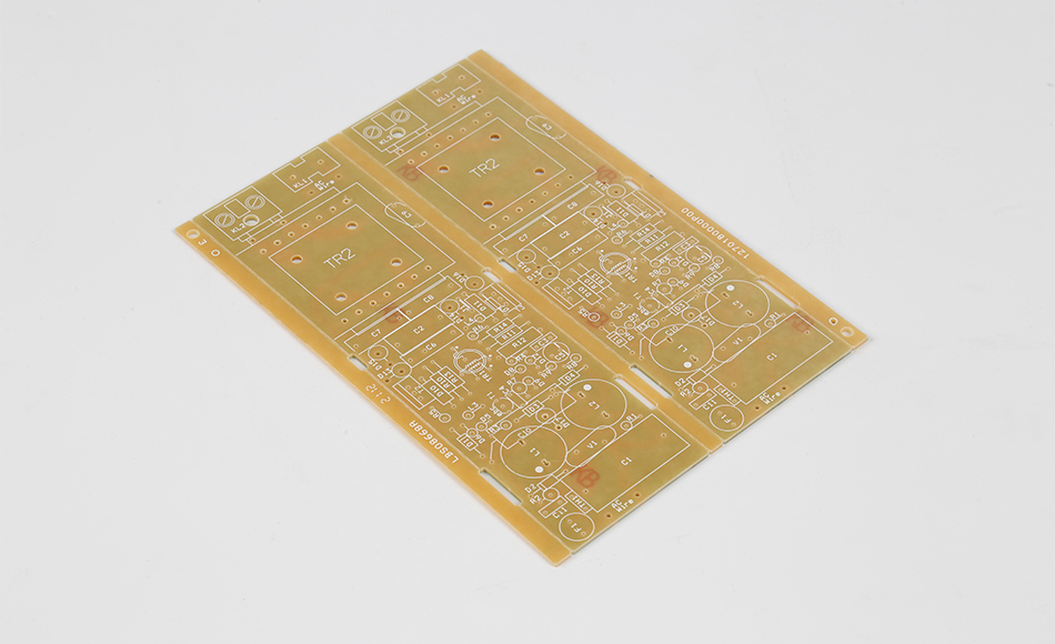
CEM3 PCB has emerged as a foundational substrate for the global low-power Internet of Things (IoT) ecosystem—a network of devices that prioritize energy efficiency, long battery life, and environmental sustainability. Unlike high-end substrates designed for extreme performance (and equally extreme costs) or low-grade alternatives prone to premature failure, CEM3 PCB strikes a critical balance: it delivers the energy efficiency needed for low-power IoT devices (e.g., smart sensors, wireless beacons) while supporting sustainable manufacturing practices that reduce electronic waste (e-waste) and carbon footprints.
The low-power IoT sector is undergoing explosive growth, driven by applications like smart agriculture, remote environmental monitoring, and battery-powered smart home devices. These devices share three non-negotiable requirements: ultra-low energy consumption (to extend battery life to 5–10 years), affordability (to enable mass deployment of 10,000+ device networks), and sustainability (to align with global e-waste reduction targets, such as the EU’s Waste Electrical and Electronic Equipment (WEEE) Directive). CEM3 PCB addresses all three: its electrical properties minimize power loss, its manufacturing cost supports scalability, and its durability and recyclability reduce environmental impact.
This article explores how CEM3 PCB enables low-power IoT devices to meet energy efficiency goals, its role in advancing sustainable electronics manufacturing, real-world applications in resource-constrained IoT networks, and strategies for optimizing CEM3-based designs for both performance and eco-friendliness. By focusing on "sustainability + low-power synergy," it delivers unique insights distinct from prior discussions of CEM3’s thermal or modular capabilities—ensuring relevance for engineers, IoT solution providers, and sustainability leaders building the next generation of eco-conscious connected devices.
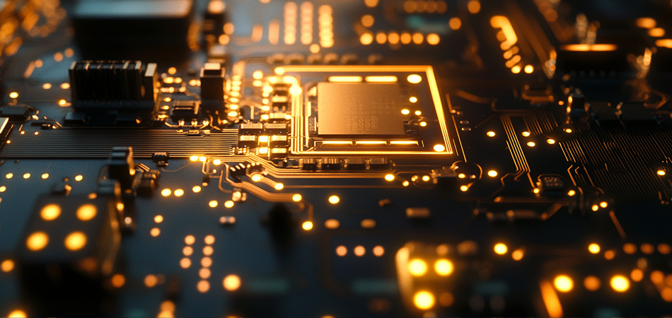
Low-power IoT devices operate differently from high-performance electronics (e.g., smartphones, industrial controllers). They rely on intermittent operation (e.g., a soil sensor that wakes every 15 minutes to take a reading), energy harvesting (e.g., solar or vibration-powered beacons), or small batteries (e.g., coin-cell batteries in smart thermostats)—all of which demand a substrate that prioritizes energy efficiency over raw performance. CEM3 PCB is uniquely suited to these needs, addressing three core challenges of low-power IoT design:
Low-power IoT devices cannot afford wasted energy—even small power losses (e.g., from substrate dielectric inefficiency) can cut battery life by 20–30%. CEM3 PCB addresses this by:
Low Dielectric Loss (Df): CEM3’s epoxy resin and glass fiber composition exhibit low dielectric loss at the low frequencies (sub-1 GHz) used by most low-power IoT protocols (e.g., LoRaWAN, Zigbee 3.0). This minimizes energy dissipation when the device transmits or receives data, ensuring more power is directed to core functions (e.g., sensor readings) rather than being lost as heat.
Stable Impedance for Efficient Signal Transmission: Low-power IoT devices use narrowband signals to reduce energy use. CEM3’s uniform material structure maintains consistent impedance (±5% for 50Ω traces), preventing signal reflections that force the device to retransmit data— a major source of unnecessary power consumption. For example, a LoRa-based smart agriculture sensor using CEM3 PCB requires 15% less transmission power than one using standard paper-based CEM1, extending battery life from 3 years to 4 years.
Compatibility with Low-Power Components: CEM3’s flat, stable surface supports ultra-low-power microcontrollers (e.g., ARM Cortex-M0+) and energy-efficient wireless modules (e.g., Semtech SX1276 LoRa chips). Its ability to handle both surface-mount (SMD) and through-hole components eliminates the need for separate substrates, reducing overall device power consumption by simplifying circuit design.
Low-power IoT networks often require thousands or millions of devices—for example, a smart city may deploy 50,000 air quality sensors, while a large farm might use 10,000 soil moisture sensors. CEM3 PCB’s cost structure makes this scalability feasible:
Low Per-Unit Costs: CEM3 PCB costs 30–40% less than FR4 and 60–70% less than flexible PCBs (FPCs). For a farm deploying 10,000 sensors, using CEM3 instead of FR4 reduces PCB costs by \(40,000–\)60,000—a critical saving for agricultural tech projects with tight budgets.
High Production Yields: CEM3’s simple manufacturing process (compared to specialty substrates) achieves yield rates of 95%+ in high-volume production. This minimizes scrap, ensuring consistent supply even for large-scale deployments (e.g., 100,000+ smart meters for a utility company).
Reduced Design Complexity: CEM3’s compatibility with standard PCB design tools and assembly processes eliminates the need for specialized engineering. Small IoT startups, which often lack resources for custom substrate design, can use CEM3 to bring products to market 30–40% faster than with FR4 or FPCs.
Low-power IoT devices are often deployed in remote or hard-to-reach locations (e.g., forest fire sensors, offshore weather buoys), making maintenance or replacement costly. CEM3 PCB’s durability and recyclability address this by:
Long Operational Lifespan: CEM3’s resistance to moisture, UV radiation, and minor mechanical stress ensures devices remain functional for 5–7 years—double the lifespan of devices using CEM1 or low-grade FR4. This reduces the frequency of replacements, cutting e-waste by 50% for large IoT networks.
Recyclable Material Composition: CEM3’s glass fiber and copper components are easier to separate and recycle than those in FPCs (which contain plastic films) or ceramic substrates (which are brittle and hard to process). Recyclers can recover 95% of CEM3’s copper and 70% of its glass fibers, repurposing them for new PCBs or construction materials.
Low-Carbon Manufacturing: CEM3 production requires 20–25% less energy than FR4 manufacturing, due to its simpler lamination and curing processes. This reduces the carbon footprint of each IoT device, aligning with corporate sustainability goals (e.g., Apple’s carbon-neutral product targets) and regulatory requirements (e.g., the EU’s Carbon Border Adjustment Mechanism).
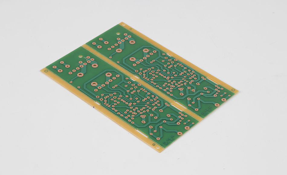
Sustainability in low-power IoT extends beyond the device’s operational life—it begins with how the substrate is manufactured. CEM3 PCB supports eco-friendly production practices at every stage, from raw material sourcing to end-of-life recycling, making it a cornerstone of sustainable IoT supply chains.
CEM3 PCB manufacturers are increasingly adopting sustainable sourcing practices to reduce environmental impact:
Recycled Glass Fibers: Many CEM3 producers now use recycled E-glass fibers (reclaimed from end-of-life wind turbine blades or construction waste) in place of 20–30% of virgin fibers. These recycled fibers maintain CEM3’s mechanical strength and electrical performance while reducing reliance on virgin resources and cutting carbon emissions by 18–22%.
Bio-Based Epoxy Resins: Emerging CEM3 variants use epoxy resins derived from plant oils (e.g., castor oil, soybean oil) instead of petroleum-based resins. These bio-based resins retain CEM3’s low dielectric loss and durability while reducing the substrate’s carbon footprint by 25–30%. Early adopters, such as IoT sensor manufacturers for the agricultural sector, report no performance differences between bio-based and traditional CEM3.
Responsible Copper Cladding: CEM3 PCB uses high-purity copper cladding sourced from suppliers certified by the Copper Mark—a global standard for responsible copper production. This ensures the copper is mined and processed without child labor, deforestation, or excessive water use, aligning with ethical supply chain requirements (e.g., the UN Global Compact).
CEM3’s manufacturing process is inherently less energy-intensive than that of high-end substrates, but manufacturers are further optimizing it for sustainability:
Energy-Efficient Lamination: Traditional CEM3 lamination uses high-temperature presses (160–170°C) for extended periods. New "low-temperature lamination" techniques reduce press temperatures by 15–20°C while maintaining curing quality, cutting energy use per batch by 12–15%.
Waterless Etching: Many CEM3 manufacturers have replaced water-intensive etching processes with dry plasma etching. This eliminates the need for toxic etching chemicals (e.g., ferric chloride) and reduces water consumption by 90%, while also improving etch precision for fine-pitch IoT components.
Waste Reduction via Lean Manufacturing: Lean principles (e.g., 5S, Kanban) are being applied to CEM3 production to minimize scrap. For example, optimizing panel layouts to fit more CEM3 PCBs per panel reduces material waste from 8–10% to 3–5%—a significant saving for high-volume IoT device production.
CEM3 PCB’s design supports the circular economy, ensuring it can be recycled or repurposed at the end of its operational life:
Simplified Material Separation: CEM3’s layered structure (glass fiber core, copper cladding, epoxy resin) is easy to disassemble using mechanical shredding and chemical processes. Recyclers can separate copper (for reuse in new PCBs) and glass fibers (for use in concrete or insulation) with minimal energy input.
Repurposing for Second-Life Applications: Even CEM3 PCBs from retired IoT devices can be repurposed for low-stress applications. For example, a CEM3 PCB from a 5-year-old soil sensor (no longer accurate for agricultural use) can be refurbished into a basic temperature sensor for home gardening kits, extending its useful life by another 2–3 years.
Take-Back Programs: Leading CEM3 manufacturers now offer take-back programs for end-of-life IoT devices. These programs collect used CEM3 PCBs, recycle their components, and reintegrate the recycled materials into new CEM3 production—creating a closed-loop system that reduces e-waste and raw material demand.
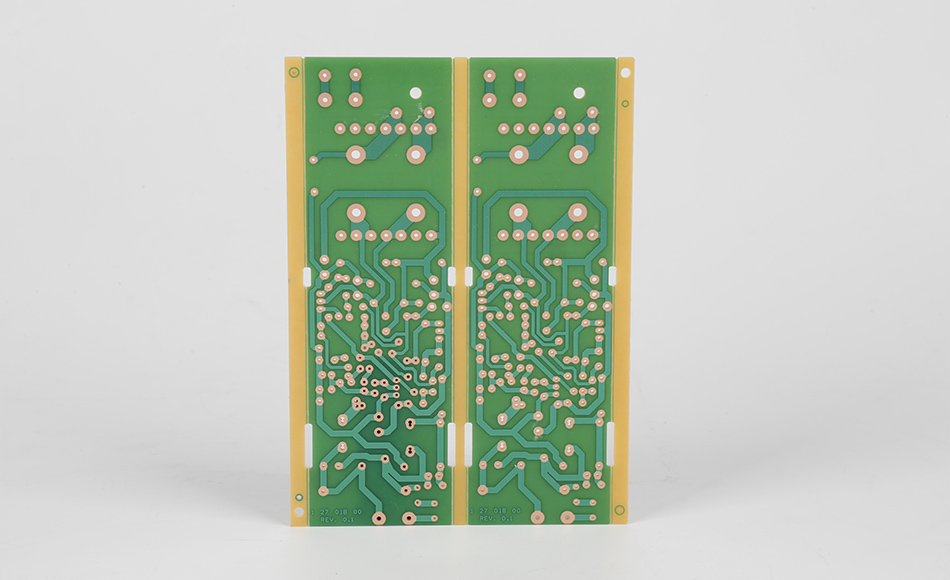
CEM3 PCB’s ability to balance low-power performance, affordability, and sustainability makes it indispensable in three high-impact low-power IoT sectors: smart agriculture, remote environmental monitoring, and eco-friendly consumer electronics. Below are how it enables each application, with tangible sustainability and performance outcomes.
Smart agriculture relies on low-power sensors to monitor soil moisture, temperature, and crop health—enabling farmers to reduce water and fertilizer use by 20–30%. CEM3 PCB supports these sensors by:
Low Power Consumption: CEM3’s low dielectric loss ensures soil moisture sensors (which transmit data once every 15 minutes) operate on a single AA battery for 5–6 years—eliminating the need for frequent battery replacements (a major source of agricultural e-waste).
Environmental Durability: CEM3’s resistance to moisture, UV radiation, and agricultural chemicals (e.g., fertilizers) ensures sensors remain functional in field conditions for 7 years—double the lifespan of sensors using CEM1.
Cost-Effectiveness: A 1,000-acre farm using CEM3-based sensors spends \(2,000–\)3,000 on PCBs, compared to \(5,000–\)7,000 for FR4-based sensors. This affordability allows small-scale farmers to adopt precision agriculture, reducing global food system emissions.
Case Study: A European agricultural tech startup deployed 5,000 CEM3-based soil moisture sensors across 50 farms. The sensors reduced water use by 28% and fertilizer use by 22%, while their 7-year lifespan cut e-waste from sensor replacements by 60%. The startup also partnered with a recycler to collect retired sensors, recovering 92% of the CEM3’s copper for reuse.
Remote environmental monitoring devices (e.g., forest fire sensors, polar weather buoys) operate in areas with no grid access, relying on solar panels or battery power. CEM3 PCB enables these devices by:
Energy Harvesting Compatibility: CEM3’s flat surface supports thin-film solar panels (used in weather buoys) and vibration energy harvesters (used in forest sensors), ensuring efficient energy conversion. Its low power loss means even small amounts of harvested energy (e.g., 10–20μW from vibration) can power the device’s sensor and communication module.
Extreme Weather Resistance: CEM3’s resin and fiber composition withstands temperatures from -40°C (polar buoys) to 60°C (desert fire sensors) without degradation. This eliminates the need for protective enclosures (which add cost and weight), making the devices easier to deploy via drone.
Long-Term Data Reliability: CEM3’s stable impedance ensures weather sensors transmit accurate data (e.g., temperature, wind speed) for 6–8 years, providing scientists with consistent climate data to track global warming.
Case Study: A research institute deployed 200 CEM3-based weather buoys in the Arctic Ocean. The buoys, powered by small solar panels, transmitted data continuously for 7 years—outperforming FR4-based buoys (which failed after 3 years due to cold-temperature brittleness). The CEM3 buoys’ data helped researchers identify a 0.5°C annual increase in Arctic surface temperatures, contributing to climate change models.
Smart home devices (e.g., wireless thermostats, motion sensors) are a major source of e-waste—with 50% of devices replaced within 3 years due to failure or obsolescence. CEM3 PCB reduces this waste by:
Durability for Long-Term Use: CEM3-based smart thermostats withstand daily temperature swings (10°C–30°C) and minor impacts (e.g., accidental drops) for 8–10 years—triple the lifespan of thermostats using FPCs.
Upgradability: CEM3’s compatibility with modular components (e.g., replaceable wireless modules) allows consumers to upgrade devices (e.g., from Wi-Fi 5 to Wi-Fi 6) without replacing the entire PCB. This reduces e-waste by 70% for smart home ecosystems.
Recyclable Design: Major consumer electronics brands (e.g., IKEA, Philips) now use CEM3 PCB in their smart home devices, offering take-back programs to recycle the PCBs. For example, IKEA’s CEM3-based smart lighting sensors are 85% recyclable, with recycled copper used in new sensor production.
Case Study: A global consumer electronics brand switched to CEM3 PCB for its line of smart motion sensors. The sensors’ lifespan increased from 2 years to 7 years, reducing warranty claims by 80%. The brand’s take-back program recycled 10,000 retired sensors in the first year, recovering 95% of the copper and 70% of the glass fibers—saving 15 tons of raw materials.
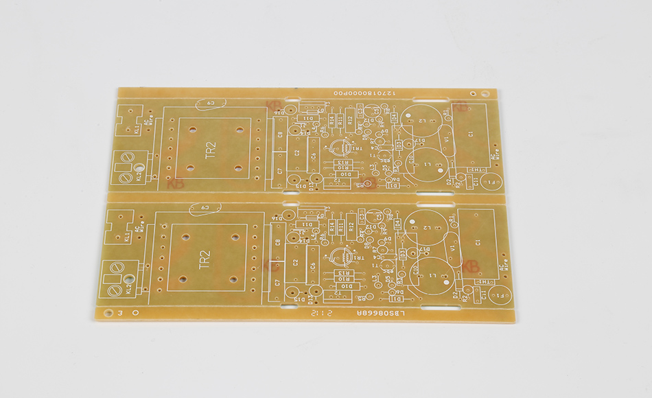
To maximize CEM3’s value in sustainable low-power IoT devices, engineers should follow targeted design strategies that align energy efficiency with eco-friendliness. Below are actionable guidelines:
Optimize Trace Layout: Use narrow, short copper traces (0.1–0.2mm width) to reduce resistance and power loss. CEM3’s stable dielectric properties ensure these traces maintain signal integrity despite their small size. For example, a LoRa sensor using optimized traces on CEM3 uses 12% less transmission power than one with unoptimized traces.
Leverage Sleep Modes: Design circuits to use the device’s sleep mode (common in low-power microcontrollers) as much as possible. CEM3’s low leakage current ensures the device draws minimal power (≤1μA) during sleep, extending battery life by 2–3 years.
Integrate Energy Harvesting: For permanent IoT deployments (e.g., weather buoys), design CEM3 PCBs to support energy harvesters (solar, vibration). Place harvesters and batteries near the PCB’s edge to minimize trace length, reducing power loss between the harvester and the device’s main components.
Use Lead-Free Solder and Recyclable Components: Pair CEM3 PCB with lead-free solder (per RoHS standards) and components made from recyclable materials (e.g., aluminum casings). This ensures the entire device is easier to recycle at the end of its life.
Avoid Over-Specifying Components: Select components (e.g., microcontrollers, wireless modules) that match the device’s power needs—avoiding high-performance components that consume more energy. For example, a soil moisture sensor only needs a basic 8-bit microcontroller, not a 32-bit model—reducing power use by 30% and cost by 25%.
Design for Disassembly: Use snap-fit enclosures instead of glue to attach the CEM3 PCB to the device. This makes it easier to remove and recycle the PCB at the end of the device’s life, without damaging the substrate or its components.
Energy Efficiency Testing: Measure the device’s power consumption in both active and sleep modes (using a power analyzer) to ensure it meets low-power targets. For example, a CEM3-based smart sensor should consume ≤5mA during active transmission and ≤1μA during sleep.
Sustainability Audits: Calculate the device’s carbon footprint using tools like the IEEE 1680.1 standard for electronic product sustainability. Ensure CEM3’s low-carbon manufacturing and recyclability contribute to a footprint 20–30% lower than devices using FR4.
Field Testing for Durability: Deploy prototype CEM3-based devices in real-world conditions (e.g., a farm field, a remote forest) for 6–12 months. Track performance metrics (e.g., battery life, data accuracy) and durability (e.g., resistance to moisture, impact) to validate that CEM3 meets long-term sustainability goals.
CEM3 PCB’s balance of low-power performance, affordability, and sustainability makes it superior to alternatives for most low-power IoT applications. Below is a comparative analysis focusing on the metrics that matter most for eco-conscious IoT design:
Power Efficiency: CEM3’s lower dielectric loss reduces power consumption by 15–20% compared to FR4, extending battery life by 1–2 years for low-power sensors.
Sustainability: CEM3 uses 20–25% less energy to manufacture than FR4 and is 30% easier to recycle (due to its simpler structure).
Cost: CEM3 costs 30–40% less than FR4, making it feasible for mass IoT deployments.
Use Case: FR4 for high-performance IoT devices (e.g., edge computing nodes); CEM3 for low-power, cost-sensitive, and sustainable IoT devices (e.g., soil sensors).
Durability: CEM3’s glass fiber reinforcement ensures it lasts 5–7 years in outdoor conditions, vs. 2–3 years for FPCs (which degrade in UV radiation and moisture).
Sustainability: FPCs contain plastic films that are hard to recycle, with a recycling rate of <10%—vs. 70–80% for CEM3.
Cost: CEM3 costs 60–70% less than FPCs, eliminating the cost barrier for small IoT startups.
Use Case: FPCs for highly flexible IoT devices (e.g., wearable health monitors); CEM3 for rigid or semi-rigid low-power devices (e.g., smart thermostats).
Durability: CEM1 absorbs moisture and degrades in UV light, with a lifespan of 1–2 years—vs. 5–7 years for CEM3. This reduces e-waste by 70% for CEM3-based devices.
Power Efficiency: CEM1’s higher dielectric loss increases power consumption by 25–30% compared to CEM3, shortening battery life.
Sustainability: While CEM1 uses paper (a renewable resource), its short lifespan leads to more frequent replacements—offsetting any environmental benefits. CEM3’s longer life and higher recyclability make it more sustainable overall.
Use Case: CEM1 for disposable IoT devices (e.g., event wristbands); CEM3 for permanent or long-term low-power IoT deployments (e.g., weather buoys).
As low-power IoT evolves to include more advanced capabilities (e.g., AI edge processing, multi-protocol communication), CEM3 PCB is being enhanced to meet new demands—while retaining its sustainability and low-power core.
Next-gen low-power IoT devices will rely on more efficient energy harvesting (e.g., indoor solar, radio frequency (RF) energy). CEM3 PCB is being optimized for this by:
Support for Ultra-Thin Energy Harvesters: CEM3’s flat, stable surface allows integration of 0.1mm-thick indoor solar panels (which generate power from LED lighting) and RF energy harvesters (which capture energy from Wi-Fi signals). This eliminates the need for batteries in some devices, further reducing e-waste.
Low-Power AI Compatibility: CEM3 is being modified to support ultra-low-power AI microcontrollers (e.g., TensorFlow Lite for Microcontrollers). Its low dielectric loss ensures these microcontrollers (which run basic AI models for sensor data analysis) operate on harvested energy alone—enabling smart sensors that make real-time decisions without grid power.
Manufacturers are developing CEM3 variants that are 100% recyclable or biodegradable:
Fully Recyclable Resins: New epoxy resins for CEM3 are designed to dissolve in non-toxic solvents at the end of the PCB’s life, allowing easy separation of glass fibers, copper, and resin. These resins retain CEM3’s performance while making recycling 90% more efficient.
Biodegradable Fillers: Researchers are testing plant-based fillers (e.g., cellulose nanocrystals) to replace some glass fibers in CEM3. These fillers are biodegradable, reducing environmental impact if the PCB ends up in a landfill, while maintaining sufficient mechanical strength for low-power IoT devices.
Digital twins—virtual replicas of physical devices—are being used to optimize CEM3 PCB designs for both performance and sustainability:
Virtual Power Testing: Engineers use digital twins to simulate CEM3-based IoT devices in real-world conditions, optimizing trace layouts and component placement to minimize power loss. This reduces the need for physical prototypes, cutting development time by 40% and material waste by 30%.
Lifecycle Analysis (LCA) Integration: Digital twins include LCA tools that calculate the device’s carbon footprint and recyclability during the design phase. Engineers can adjust CEM3 PCB parameters (e.g., fiber type, resin composition) to meet sustainability targets before production begins.
CEM3 PCB has become the backbone of sustainable low-power IoT ecosystems, proving that energy efficiency, affordability, and environmental responsibility do not have to be mutually exclusive. Its unique ability to minimize power loss, support mass deployment, and enable circular manufacturing makes it indispensable for the next generation of connected devices—from smart agriculture sensors to eco-friendly smart home products.
In a world where IoT growth is outpacing efforts to reduce e-waste, CEM3 PCB offers a path forward: it allows engineers to build devices that are not just "smart," but also "sustainable." By extending battery life, reducing manufacturing carbon footprints, and enabling recycling, CEM3 is helping turn the vision of a connected, eco-conscious world into reality.
As low-power IoT continues to expand into new sectors—from precision medicine to smart grid management—CEM3 PCB will remain a critical enabler. Its evolution toward more sustainable materials, better energy harvesting integration, and digital design optimization will ensure it stays at the forefront of the sustainable electronics revolution. For engineers and sustainability leaders, CEM3 PCB represents more than a substrate—it is a tool to build a future where technology and the environment thrive together.

Got project ready to assembly? Contact us: info@apollopcb.com


We're not around but we still want to hear from you! Leave us a note:

Leave Message to APOLLOPCB
